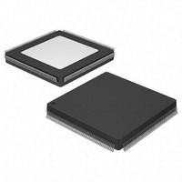
XCS30XL-4PQ208I Xilinx Inc, XCS30XL-4PQ208I Datasheet - Page 50

XCS30XL-4PQ208I
Manufacturer Part Number
XCS30XL-4PQ208I
Description
IC FPGA 3.3V I-TEMP HP 208PQFP
Manufacturer
Xilinx Inc
Series
Spartan™-XLr
Datasheet
1.XCS05XL-4VQG100C.pdf
(83 pages)
Specifications of XCS30XL-4PQ208I
Number Of Logic Elements/cells
1368
Number Of Labs/clbs
576
Total Ram Bits
18432
Number Of I /o
169
Number Of Gates
30000
Voltage - Supply
3 V ~ 3.6 V
Mounting Type
Surface Mount
Operating Temperature
-40°C ~ 100°C
Package / Case
208-BFQFP
Lead Free Status / RoHS Status
Contains lead / RoHS non-compliant
Available stocks
Company
Part Number
Manufacturer
Quantity
Price
Company:
Part Number:
XCS30XL-4PQ208I
Manufacturer:
XILINX
Quantity:
10
Company:
Part Number:
XCS30XL-4PQ208I
Manufacturer:
XILINX
Quantity:
402
Part Number:
XCS30XL-4PQ208I
Manufacturer:
ALTERA/阿尔特拉
Quantity:
20 000
Spartan and Spartan-XL FPGA Families Data Sheet
Spartan Family IOB Input Switching Characteristic Guidelines
All devices are 100% functionally tested. Internal timing
parameters are derived from measuring internal test pat-
terns. Listed below are representative values. For more
specific, more precise, and worst-case guaranteed data,
use the values reported by the static timing analyzer (TRCE
50
Notes:
1.
2.
3.
Setup Times - TTL Inputs
Hold Times
Propagation Delays - TTL Inputs
Delay Adder for Input with Delay Option
Global Set/Reset
Symbol
T
T
T
T
T
T
T
T
T
T
Delay
MRW
ECIK
PICK
IKEC
IKRI
Delay adder for CMOS Inputs option: for -3 speed grade, add 0.4 ns; for -4 speed grade, add 0.2 ns.
Input pad setup and hold times are specified with respect to the internal clock (IK). For setup and hold times with respect to the clock
input, see the pin-to-pin parameters in the Pin-to-Pin Input Parameters table.
Voltage levels of unused pads, bonded or unbonded, must be valid logic levels. Each can be configured with the internal pull-up
(default) or pull-down resistor, or configured as a driven output, or can be driven from an external source.
PID
IKLI
RRI
PLI
Clock Enable (EC) to Clock (IK), no delay
Pad to Clock (IK), no delay
Clock Enable (EC) to Clock (IK), no delay
All Other Hold Times
Pad to I1, I2
Pad to I1, I2 via transparent input latch, no delay
Clock (IK) to I1, I2 (flip-flop)
Clock (IK) to I1, I2 (latch enable, active Low)
T
T
T
Minimum GSR pulse width
Delay from GSR input to any Q
ECIKD
PICKD
PDLI
= T
= T
= T
PLI
ECIK
PICK
+ T
(1)
+ T
+ T
Delay
Delay
Delay
Description
(1)
www.xilinx.com
in the Xilinx Development System) and back-annotated to
the simulation netlist. These path delays, provided as a
guideline, have been extracted from the static timing ana-
lyzer report. All timing parameters assume worst-case oper-
ating conditions (supply voltage and junction temperature).
All devices
All devices
All devices
All devices
All devices
All devices
All devices
All devices
All devices
Device
XCS05
XCS10
XCS20
XCS30
XCS40
XCS05
XCS10
XCS20
XCS30
XCS40
11.5
Min
0.0
3.6
3.7
3.8
4.5
5.5
1.6
1.5
0.0
-
-
-
-
-
-
-
-
-
-4
Speed Grade
Max
10.0
10.5
11.0
1.5
2.8
2.7
3.2
9.0
9.5
-
-
-
-
-
-
-
-
-
-
DS060 (v1.8) June 26, 2008
13.5
Min
2.1
2.0
0.9
0.0
4.0
4.1
4.2
5.0
5.5
-
-
-
-
-
-
-
-
-
Product Specification
-3
Max
11.3
11.9
12.5
13.1
13.8
2.0
3.6
2.8
3.9
-
-
-
-
-
-
-
-
-
-
Units
ns
ns
ns
ns
ns
ns
ns
ns
ns
ns
ns
ns
ns
ns
ns
ns
ns
ns
ns
R


