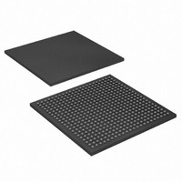
XC3SD1800A-4CS484C Xilinx Inc, XC3SD1800A-4CS484C Datasheet - Page 38

XC3SD1800A-4CS484C
Manufacturer Part Number
XC3SD1800A-4CS484C
Description
SPARTAN-3ADSP FPGA 1800K 484CSA
Manufacturer
Xilinx Inc
Series
Spartan™-3A DSPr
Datasheets
1.XC3S50A-4VQG100C.pdf
(7 pages)
2.XC3SD3400A-4FGG676C.pdf
(4 pages)
3.XC3SD3400A-4FGG676C.pdf
(101 pages)
Specifications of XC3SD1800A-4CS484C
Number Of Logic Elements/cells
37440
Number Of Labs/clbs
4160
Total Ram Bits
1548288
Number Of I /o
309
Number Of Gates
1800000
Voltage - Supply
1.14 V ~ 1.26 V
Mounting Type
Surface Mount
Operating Temperature
0°C ~ 85°C
Package / Case
484-FBGA, CSPBGA
For Use With
122-1574 - KIT DEVELOPMENT SPARTAN 3ADSP
Lead Free Status / RoHS Status
Contains lead / RoHS non-compliant
Available stocks
Company
Part Number
Manufacturer
Quantity
Price
Company:
Part Number:
XC3SD1800A-4CS484C
Manufacturer:
XILINX
Quantity:
1 045
Part Number:
XC3SD1800A-4CS484C
Manufacturer:
XILINX/赛灵思
Quantity:
20 000
Configurable Logic Block (CLB) Timing
Table 29: CLB (SLICEM) Timing
DS610 (v3.0) October 4, 2010
Product Specification
Notes:
1.
Clock-to-Output Times
T
Setup Times
T
T
Hold Times
T
T
Clock Timing
T
T
F
Propagation Times
T
Set/Reset Pulse Width
T
AS
AH
CKO
DICK
CKDI
CH
CL
TOG
ILO
RPW_CLB
The numbers in this table are based on the operating conditions set forth in
Symbol
When reading from the FFX (FFY) Flip-Flop, the time
from the active transition at the CLK input to data
appearing at the XQ (YQ) output
Time from the setup of data at the F or G input to the
active transition at the CLK input of the CLB
Time from the setup of data at the BX or BY input to
the active transition at the CLK input of the CLB
Time from the active transition at the CLK input to the
point where data is last held at the F or G input
Time from the active transition at the CLK input to the
point where data is last held at the BX or BY input
The High pulse width of the CLB’s CLK signal
The Low pulse width of the CLK signal
Toggle frequency (for export control)
The time it takes for data to travel from the CLB’s
F (G) input to the X (Y) output
The minimum allowable pulse width, High or Low, to
the CLB’s SR input
Description
Spartan-3A DSP FPGA Family: DC and Switching Characteristics
www.xilinx.com
Table
0.63
0.18
1.58
0.00
0.00
0.63
1.33
Min
–
0
–
7.
-5
Max
0.60
0.62
770
Speed Grade
–
–
–
–
–
–
–
0.36
1.88
0.00
0.00
0.75
0.75
1.61
Min
–
0
–
-4
Max
0.68
0.71
667
–
–
–
–
–
–
–
Units
MHz
ns
ns
ns
ns
ns
ns
ns
ns
ns
38


