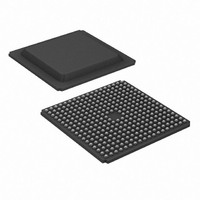
XC3S1600E-5FGG320C Xilinx Inc, XC3S1600E-5FGG320C Datasheet - Page 60

XC3S1600E-5FGG320C
Manufacturer Part Number
XC3S1600E-5FGG320C
Description
IC FPGA SPARTAN-3E 1600K 320FBGA
Manufacturer
Xilinx Inc
Series
Spartan™-3Er
Datasheet
1.XC3S100E-4VQG100C.pdf
(233 pages)
Specifications of XC3S1600E-5FGG320C
Number Of Logic Elements/cells
33192
Number Of Labs/clbs
3688
Total Ram Bits
663552
Number Of I /o
250
Number Of Gates
1600000
Voltage - Supply
1.14 V ~ 1.26 V
Mounting Type
Surface Mount
Operating Temperature
0°C ~ 85°C
Package / Case
320-BGA
For Use With
HW-XA3S1600E-UNI-G - KIT DEVELOPMENT AUTOMOTIVE ECU
Lead Free Status / RoHS Status
Lead free / RoHS Compliant
Available stocks
Company
Part Number
Manufacturer
Quantity
Price
Company:
Part Number:
XC3S1600E-5FGG320C
Manufacturer:
Xilinx Inc
Quantity:
10 000
Part Number:
XC3S1600E-5FGG320C
Manufacturer:
XILINX/赛灵思
Quantity:
20 000
Company:
Part Number:
XC3S1600E-5FGG320C/4I
Manufacturer:
XILINX
Quantity:
150
- Current page: 60 of 233
- Download datasheet (6Mb)
Functional Description
60
Notes:
1.
2.
3.
4.
5.
6.
The diagram presents electrical connectivity. The diagram locations do not necessarily match the physical location on the device,
although the coordinate locations shown are correct.
Number of DCMs and locations of these DCM varies for different device densities. The left and right DCMs are only in the
XC3S1200E and XC3S1600E. The XC3S100E has only two DCMs, one on the top right and one on the bottom right of the die.
See
See
For best direct clock inputs to a particular clock buffer, not a DCM, see
For best direct clock inputs to a particular DCM, not a BUFGMUX, see
are shown in gray.
XC3S1200E (X0Y2)
XC3S1600E (X0Y2)
2
XC3S1200E (X0Y1)
XC3S1600E (X0Y1)
2
2
2
BUFGMUX
BUFGMUX
Figure
Figure
DCM
DCM
pair
Figure 45: Spartan-3E Internal Quadrant-Based Clock Network (Electrical Connectivity View)
47a, which shows how the eight clock lines are multiplexed on the left-hand side of the device.
47b, which shows how the eight clock lines are multiplexed on the right-hand side of the device.
2
2
2
2
G
A
H
E
C
B
F
D
Bottom Left
Quadrant (BL)
Top Left
Quadrant (TL)
Left Spine
8
8
XC3S1200E (X1Y3)
XC3S1600E (X1Y3)
XC3S1200E (X1Y0)
XC3S1600E (X1Y0)
XC3S250E (X0Y1)
XC3S500E (X0Y1)
XC3S250E (X0Y0)
XC3S500E (X0Y0)
DCM
DCM
8
Note 3
Note 3
•
•
•
•
•
•
8
8
8
8
4
4
4
8
4
GCLK11
GCLK3
X1Y10 X1Y11
X1Y0 X1Y1
GCLK7
GCLK15
Global Clock Inputs
H
D
Horizontal
GCLK2
Global Clock Inputs
GCLK10
www.xilinx.com
GCLK6
GCLK14
G
C
4
GCLK9
4
GCLK1
X2Y10 X2Y11
X2Y0 X2Y1
GCLK13
GCLK5
B
F
Spine
GCLK0
GCLK8
GCLK12
Table
GCLK4
Table
E
A
4
4
30,
8
41.
4
4
Table
XC3S1200E (X2Y3)
XC3S1600E (X2Y3)
XC3S1200E (X2Y0)
XC3S1600E (X2Y0)
XC3S100E (X0Y1)
XC3S250E (X1Y1)
XC3S500E (X1Y1)
XC3S100E (X0Y0)
XC3S250E (X1Y0)
XC3S500E (X1Y0)
Note 4
Note 4
•
•
•
•
•
•
8
8
8
8
DCM
DCM
31, and
8
Quadrant (TR)
Quadrant (BR)
Bottom Right
Table
Right Spine
Top Right
DS312-2 (v3.8) August 26, 2009
32. Direct pin inputs to a DCM
8
8
Product Specification
in Quadrant
Clock Line
XC3S1200E (X3Y1)
XC3S1600E (X3Y1)
XC3S1200E (X3Y2)
XC3S1600E (X3Y2)
2
2
2
2
H
G
E
C
B
A
F
D
DS312-2_04_041106
DCM
DCM
2
2
2
2
R
Related parts for XC3S1600E-5FGG320C
Image
Part Number
Description
Manufacturer
Datasheet
Request
R

Part Number:
Description:
IC SPARTAN-3E FPGA 1600K 320-FBG
Manufacturer:
Xilinx Inc
Datasheet:

Part Number:
Description:
IC SPARTAN-3E FPGA 1600K 400FBGA
Manufacturer:
Xilinx Inc
Datasheet:

Part Number:
Description:
IC FPGA SPARTAN-3E 1600K 320FBGA
Manufacturer:
Xilinx Inc
Datasheet:

Part Number:
Description:
IC FPGA SPARTAN-3E 1600K 400FBGA
Manufacturer:
Xilinx Inc
Datasheet:

Part Number:
Description:
IC FPGA SPARTAN-3E 1600K 484FBGA
Manufacturer:
Xilinx Inc
Datasheet:

Part Number:
Description:
IC FPGA SPARTAN 3E 320FBGA
Manufacturer:
Xilinx Inc
Datasheet:

Part Number:
Description:
IC FPGA SPARTAN 3E 400FBGA
Manufacturer:
Xilinx Inc
Datasheet:

Part Number:
Description:
IC FPGA SPARTAN 3E 484FBGA
Manufacturer:
Xilinx Inc
Datasheet:

Part Number:
Description:
FPGA, SPARTAN-3E, 1600K GATES, 484FBGA
Manufacturer:
Xilinx Inc
Datasheet:

Part Number:
Description:
PROGRAMMABLE MICROCHIP
Manufacturer:
Xilinx Inc
Datasheet:

Part Number:
Description:
FPGA Spartan®-3E Family 1.6M Gates 33192 Cells 572MHz 90nm (CMOS) Technology 1.2V 484-Pin FBGA
Manufacturer:
Xilinx Inc
Datasheet:

Part Number:
Description:
FPGA Spartan®-3E Family 1.6M Gates 33192 Cells 657MHz 90nm (CMOS) Technology 1.2V 400-Pin FBGA
Manufacturer:
Xilinx Inc
Datasheet:

Part Number:
Description:
FPGA Spartan®-3E Family 1.6M Gates 33192 Cells 657MHz 90nm (CMOS) Technology 1.2V 400-Pin FBGA
Manufacturer:
Xilinx Inc
Datasheet:

Part Number:
Description:
FPGA Spartan®-3E Family 1.6M Gates 33192 Cells 572MHz 90nm (CMOS) Technology 1.2V 320-Pin FBGA
Manufacturer:
Xilinx Inc
Datasheet:

Part Number:
Description:
IC CPLD .8K 36MCELL 44-VQFP
Manufacturer:
Xilinx Inc
Datasheet:


