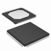
XCV50-5TQ144I Xilinx Inc, XCV50-5TQ144I Datasheet - Page 34

XCV50-5TQ144I
Manufacturer Part Number
XCV50-5TQ144I
Description
IC FPGA 2.5V I-TEMP 144-TQFP
Manufacturer
Xilinx Inc
Series
Virtex™r
Datasheet
1.XCV100-5PQ240C.pdf
(76 pages)
Specifications of XCV50-5TQ144I
Number Of Logic Elements/cells
1728
Number Of Labs/clbs
384
Total Ram Bits
32768
Number Of I /o
98
Number Of Gates
57906
Voltage - Supply
2.375 V ~ 2.625 V
Mounting Type
Surface Mount
Operating Temperature
-40°C ~ 100°C
Package / Case
144-LQFP
Lead Free Status / RoHS Status
Contains lead / RoHS non-compliant
Available stocks
Company
Part Number
Manufacturer
Quantity
Price
Company:
Part Number:
XCV50-5TQ144I
Manufacturer:
XILINX
Quantity:
988
Virtex™ 2.5 V Field Programmable Gate Arrays
Calculation of T
Capacitance
T
the pad. The values for T
capacitive load (Csl) for each I/O standard as listed in
Table
Table 2: Constants for Calculating T
Module 3 of 4
10
Notes:
1.
2.
LVTTL Fast Slew Rate, 2mA drive
LVTTL Fast Slew Rate, 4mA drive
LVTTL Fast Slew Rate, 6mA drive
LVTTL Fast Slew Rate, 8mA drive
LVTTL Fast Slew Rate, 12mA drive
LVTTL Fast Slew Rate, 16mA drive
LVTTL Fast Slew Rate, 24mA drive
LVTTL Slow Slew Rate, 2mA drive
LVTTL Slow Slew Rate, 4mA drive
LVTTL Slow Slew Rate, 6mA drive
LVTTL Slow Slew Rate, 8mA drive
LVTTL Slow Slew Rate, 12mA drive
LVTTL Slow Slew Rate, 16mA drive
LVTTL Slow Slew Rate, 24mA drive
LVCMOS2
PCI 33MHz 5V
PCI 33MHZ 3.3 V
PCI 66 MHz 3.3 V
GTL
GTL+
HSTL Class I
HSTL Class III
HSTL Class IV
SSTL2 Class I
SSTL2 Class II
SSTL3 Class I
SSTL3 Class II
CTT
AGP
ioop
I/O parameter measurements are made with the capacitance
values shown above. See Application Note XAPP133 on
www.xilinx.com
I/O standard measurements are reflected in the IBIS model
information except where the IBIS format precludes it.
is the propagation delay from the O Input of the IOB to
2.
Standard
for appropriate terminations.
ioop
as a Function of
ioop
were based on the standard
ioop
(pF)
Csl
35
35
35
35
35
35
35
35
35
35
35
35
35
35
35
50
10
10
20
20
20
30
30
30
30
20
10
0
0
(ns/pF)
0.079
0.044
0.043
0.033
0.100
0.086
0.058
0.050
0.048
0.041
0.050
0.050
0.033
0.014
0.017
0.022
0.016
0.014
0.035
0.037
0.028
0.016
0.029
0.016
0.41
0.20
0.13
0.41
0.20
fl
www.xilinx.com
1-800-255-7778
For other capacitive loads, use the formulas below to calcu-
late the corresponding T
Where:
Table 3: Delay Measurement Methodology
Notes:
1.
2.
3.
4.
LVTTL
LVCMOS2
PCI33_5
PCI33_3
PCI66_3
GTL
GTL+
HSTL Class I
HSTL Class III
HSTL Class IV
SSTL3 I & II
SSTL2 I & II
CTT
AGP
Standard
T
T
Adjustment section.
C
Input waveform switches between V
Measurements are made at VREF (Typ), Maximum, and
Minimum. Worst-case values are reported.
I/O parameter measurements are made with the capacitance
values shown in
www.xilinx.com
I/O standard measurements are reflected in the IBIS model
information except where the IBIS format precludes it.
opadjust
ioop
load
= T
is the capacitive load for the design.
is reported above in the Output Delay
ioop
+ T
V
(0.2xV
V
V
V
V
V
V
V
REF
Table
REF
REF
REF
REF
REF
REF
REF
V
opadjust
V
for appropriate terminations.
REF
L
0
0
–0.75
(1)
–0.2
–0.2
–0.5
–0.5
–0.5
–1.0
–0.2
CCO
ioop
2. See Application Note XAPP133 on
–
DS003-3 (v3.2) September 10, 2002
Production Product Specification
+ (C
Per PCI Spec
Per PCI Spec
Per PCI Spec
)
.
V
(0.2xV
V
V
V
V
V
V
V
load
REF
REF
REF
REF
REF
REF
REF
REF
V
V
REF
2.5
H
3
– C
+0.75
(1)
+0.2
+0.2
+0.5
+0.5
+0.5
+1.0
+0.2
CCO
L
+
and V
sl
)
) * fl
H
Meas.
Point
1.125
V
V
V
V
V
V
V
V
V
.
1.4
REF
REF
REF
REF
REF
REF
REF
REF
REF
Typ
V
Spec
AGP
0.80
0.75
0.90
0.90
1.25
Per
1.0
1.5
1.5
REF
-
-
-
-
-
(2)
R


