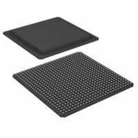
XC2V3000-5FGG676I Xilinx Inc, XC2V3000-5FGG676I Datasheet - Page 79

XC2V3000-5FGG676I
Manufacturer Part Number
XC2V3000-5FGG676I
Description
IC FPGA VIRTEX-II 3M 676-FBGA
Manufacturer
Xilinx Inc
Series
Virtex™-IIr
Datasheet
1.XC2V250-4FGG256C.pdf
(318 pages)
Specifications of XC2V3000-5FGG676I
Number Of Labs/clbs
3584
Total Ram Bits
1769472
Number Of I /o
484
Number Of Gates
3000000
Voltage - Supply
1.425 V ~ 1.575 V
Mounting Type
Surface Mount
Operating Temperature
-40°C ~ 100°C
Package / Case
676-BBGA
Dc
06+
Lead Free Status / RoHS Status
Lead free / RoHS Compliant
Number Of Logic Elements/cells
-
Available stocks
Company
Part Number
Manufacturer
Quantity
Price
Company:
Part Number:
XC2V3000-5FGG676I
Manufacturer:
XILINX
Quantity:
1 831
Company:
Part Number:
XC2V3000-5FGG676I
Manufacturer:
Xilinx Inc
Quantity:
10 000
- Current page: 79 of 318
- Download datasheet (3Mb)
Virtex-II Pin-to-Pin Output Parameter Guidelines
All devices are 100% functionally tested. Listed below are representative values for typical pin locations and normal clock
loading. Values are expressed in nanoseconds unless otherwise noted.
Global Clock Input to Output Delay for LVTTL, 12 mA, Fast Slew Rate, With DCM
Table 34: Global Clock Input to Output Delay for LVTTL, 12 mA, Fast Slew Rate, With DCM
DS031-3 (v3.5) November 5, 2007
Product Specification
Notes:
1. Listed above are representative values where one global clock input drives one vertical clock line in each accessible column, and
2. Output timing is measured at 50% V
LVTTL Global Clock Input to Output delay using
Output flip-flop, 12 mA, Fast Slew Rate, with
DCM.
For data output with different standards, adjust
the delays with the values shown in
Switching Characteristics Standard
Adjustments, page
Global Clock and OFF with DCM
where all accessible IOB and CLB flip-flops are clocked by the global clock net.
R
Description
14.
IOB Output
CC
threshold with test setup shown in
T
Symbol
ICKOFDCM
www.xilinx.com
Virtex-II Platform FPGAs: DC and Switching Characteristics
XC2V1000
XC2V1500
XC2V2000
XC2V3000
XC2V4000
XC2V6000
XC2V8000
XC2V250
XC2V500
XC2V40
XC2V80
Device
Figure
1. For other I/O standards, see
1.10
1.10
1.10
1.10
1.10
1.10
1.10
1.19
1.19
1.64
-6
Speed Grade
1.28
1.28
1.28
1.28
1.28
1.28
1.28
1.38
1.38
1.88
1.88
-5
Table
1.48
1.48
1.48
1.48
1.48
1.48
1.48
1.59
1.59
2.17
2.17
-4
Module 3 of 4
19.
Units
ns
ns
ns
ns
ns
ns
ns
ns
ns
ns
ns
31
Related parts for XC2V3000-5FGG676I
Image
Part Number
Description
Manufacturer
Datasheet
Request
R

Part Number:
Description:
IC VIRTEX-II FPGA 3M 676-FBGA
Manufacturer:
Xilinx Inc
Datasheet:

Part Number:
Description:
IC VIRTEX-II FPGA 3M 1152-FCBGA
Manufacturer:
Xilinx Inc
Datasheet:

Part Number:
Description:
IC FPGA VIRTEX II 3M 957-FCBGA
Manufacturer:
Xilinx Inc
Datasheet:

Part Number:
Description:
IC FPGA VIRTEX-II 3M 676-FBGA
Manufacturer:
Xilinx Inc
Datasheet:

Part Number:
Description:
IC FPGA VIRTEX II 3M 957-FCBGA
Manufacturer:
Xilinx Inc
Datasheet:

Part Number:
Description:
IC FPGA VIRTEX-II 3M 1152-FBGA
Manufacturer:
Xilinx Inc
Datasheet:

Part Number:
Description:
IC FPGA VIRTEX-II 3M 1152-FBGA
Manufacturer:
Xilinx Inc
Datasheet:

Part Number:
Description:
IC FPGA VIRTEX-II 3M 676-FBGA
Manufacturer:
Xilinx Inc
Datasheet:

Part Number:
Description:
IC FPGA VIRTEX-II 3M 1152-FBGA
Manufacturer:
Xilinx Inc
Datasheet:

Part Number:
Description:
IC FPGA VIRTEX-II 3M 1152-FBGA
Manufacturer:
Xilinx Inc
Datasheet:

Part Number:
Description:
IC FPGA VIRTEX-II 676FGBGA
Manufacturer:
Xilinx Inc
Datasheet:

Part Number:
Description:
IC FPGA VIRTEX-II 728PBGA
Manufacturer:
Xilinx Inc
Datasheet:

Part Number:
Description:
IC FPGA VIRTEX-II 1152FCBGA
Manufacturer:
Xilinx Inc
Datasheet:

Part Number:
Description:
IC FPGA VIRTEX-II 957FCBGA
Manufacturer:
Xilinx Inc
Datasheet:

Part Number:
Description:
IC FPGA VIRTEX-II 957FCBGA
Manufacturer:
Xilinx Inc
Datasheet:


