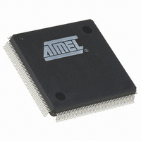
AT40K40AL-1DQC Atmel, AT40K40AL-1DQC Datasheet - Page 11

AT40K40AL-1DQC
Manufacturer Part Number
AT40K40AL-1DQC
Description
IC FPGA 40K GATES 208PQFP
Manufacturer
Atmel
Series
AT40KALr
Specifications of AT40K40AL-1DQC
Number Of Logic Elements/cells
2304
Total Ram Bits
18432
Number Of I /o
161
Number Of Gates
50000
Voltage - Supply
3 V ~ 3.6 V
Mounting Type
Surface Mount
Operating Temperature
0°C ~ 70°C
Package / Case
208-BFQFP
Lead Free Status / RoHS Status
Contains lead / RoHS non-compliant
Number Of Labs/clbs
-
Other names
AT40K40AL1DQC
RAM
2818F–FPGA–07/06
32 x 4 dual-ported RAM blocks are dispersed throughout the array, see Figure 7. A 4-bit
Input Data Bus connects to four horizontal local buses distributed over four sector rows
(plane 1). A 4-bit Output Data Bus connects to four horizontal local buses distributed
over four sector rows (plane 2). A 5-bit Input Address Bus connects to five vertical
express buses in the same column. A 5-bit Output Address Bus connects to five vertical
express buses in the same column. Ain (input address) and Aout (output address)
alternate positions in horizontally aligned RAM blocks. For the left-most RAM blocks,
Aout is on the left and Ain is on the right. For the right-most RAM blocks, Ain is on the
left and Aout is tied off, thus it can only be configured as a single port. For single-ported
RAM, Ain is the READ/WRITE address port and Din is the (bi-directional) data port.
Right-most RAM blocks can be used only for single-ported memories. WEN and OEN
connect to the vertical express buses in the same column.
Figure 7. RAM Connections (One Ram Block)
AT40KAL Series FPGA
CLK
CLK
CLK
CLK
Ain
WEN
OEN
32 x 4 RAM
Din
CLK
Dout
Aout
11


