30064 Parallax Inc, 30064 Datasheet - Page 10
30064
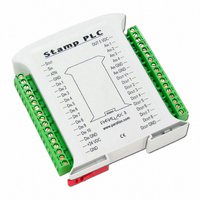
Manufacturer Part Number
30064
Description
STAMP PLC
Manufacturer
Parallax Inc
Datasheet
1.30064.pdf
(27 pages)
Specifications of 30064
Product
Microcontroller Accessories
Lead Free Status / RoHS Status
Lead free / RoHS Compliant
For Use With/related Products
BASIC Stamp®
Module/board Type
-
Lead Free Status / RoHS Status
Lead free / RoHS Compliant, Lead free / RoHS Compliant
Other names
Q2172565


The A/D Converter is configured by sending it a control byte. The control byte is made up of
configuration bits
The entire process of configuring the ADC and retrieving the conversion results can be accomplished with
just a few PBASIC commands. The following program has been written to configure the ADC for 0-5 VDC
and read the analog voltage present at Ain 2.
'{$STAMP
'{$PBASIC 2.5}
'
ClkAdc
CsAdc
AoutAdc
AinAdc
adResult
Main:
The LOW CsAdc command sets the Chip Select input of the ADC low, thereby enabling communications
on the ADC. The SHIFTOUT command sends the configuration to the ADC. The "HIGH CSadc" signals
the completion of the configuration and the start of the data conversion. The data conversion process
requires at least 9.09 uSec to complete. Since the inter-instruction time for all Stamps is higher than this,
no additional delay is required. The next "LOW CDadc" command enables communication for the reply.
The SHIFTIN command retrieves the converted data. The following "HIGH CSadc" command ends the
communications. The DEBUG command formats and displays the data for our viewing ease.
4
select bits is a subtle hint. Analog input channels 1:4 are mapped to A/D converter channels 7:4. It was decided to limit the number of analog input
channels to accommodate the number of connections available in this small enclosure.
Parallax, Inc. • Stamp PLC (#30064) • Version 1.8 • 12/29/2003
You may have noticed that the MAX1270 is an 8 channel A/D converter, (yet only 4 channels are employed). The fact that there are three channel
DO
LOOP
LOW CsAdc
SHIFTOUT AoutAdc, ClkAdc, MSBFIRST, [%11100000]
HIGH CsAdc
LOW CsAdc
SHIFTIN AinAdc, ClkAdc, MSBPRE, [adResult\12]
HIGH CsAdc
DEBUG "
BS2}
Figure 11: A/D Converter
ADC2:", SDEC adResult, CR
4
Channel
. The meaning of each configuration bit is defined by the chart in Figure 10.
Analog
4
3
2
1
Start
PIN
PIN
PIN
PIN
VAR
Bit7
1
bit table
Figure 10: A/D Converter control byte legend
SEL2
Bit6
1
W
0
3
4
5
Word
0
0
1
1
SEL1
Bit5
W
X
0
1
0
1
SEL0
Bit4
X
' A/D clock
' Chip Select for ADC
' A/D Data out
' A/D Data in
Y
0
0
1
1
Figure 12: A/D Converter bit table
RNG
Bit3
Y
Z
0
1
0
1
Bit2
BIP
Z
'Ch2 0-5 VDC
-10 VDC to +10 VDC
-5 VDC to +5 VDC
0 VDC to +10VDC
0 VDC to +5 VDC
Bit1
PD1
0
Range
PD0
Bit0
0
Page
10
Related parts for 30064
Image
Part Number
Description
Manufacturer
Datasheet
Request
R


Part Number:
Description:
Microcontroller Modules & Accessories DISCONTINUED BY PARALLAX
Manufacturer:
Parallax Inc

Part Number:
Description:
BOOK UNDERSTANDING SIGNALS
Manufacturer:
Parallax Inc
Datasheet:


Part Number:
Description:
COMPETITION RING FOR SUMOBOT
Manufacturer:
Parallax Inc
Datasheet:


Part Number:
Description:
TEXT INFRARED REMOTE FOR BOE-BOT
Manufacturer:
Parallax Inc
Datasheet:
Part Number:
Description:
BOARD EXPERIMENT+LCD NX-1000
Manufacturer:
Parallax Inc
Datasheet:

Part Number:
Description:
CONTROLLER 16SERVO MOTOR CONTROL
Manufacturer:
Parallax Inc
Datasheet:

Part Number:
Description:
BASIC STAMP LOGIC ANALYZER
Manufacturer:
Parallax Inc
Datasheet:

Part Number:
Description:
IC MCU 2K FLASH 50MHZ SO-18
Manufacturer:
Parallax Inc
Datasheet: