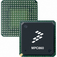
MPC859TVR133A Freescale Semiconductor, MPC859TVR133A Datasheet - Page 76

MPC859TVR133A
Manufacturer Part Number
MPC859TVR133A
Description
IC MPU POWERQUICC 133MHZ 357PBGA
Manufacturer
Freescale Semiconductor
Datasheet
1.MPC859DSLCVR50A.pdf
(96 pages)
Specifications of MPC859TVR133A
Processor Type
MPC8xx PowerQUICC 32-Bit
Speed
133MHz
Voltage
1.8V
Mounting Type
Surface Mount
Package / Case
357-PBGA
Processor Series
MPC8xx
Core
MPC8xx
Data Bus Width
32 bit
Maximum Clock Frequency
133 MHz
Maximum Operating Temperature
+ 95 C
Mounting Style
SMD/SMT
Minimum Operating Temperature
0 C
Family Name
MPC8xx
Device Core
PowerQUICC
Device Core Size
32b
Frequency (max)
133MHz
Instruction Set Architecture
RISC
Supply Voltage 1 (typ)
1.8V
Operating Supply Voltage (max)
1.9V
Operating Supply Voltage (min)
1.7V
Operating Temp Range
0C to 95C
Operating Temperature Classification
Commercial
Mounting
Surface Mount
Pin Count
357
Package Type
BGA
Lead Free Status / RoHS Status
Lead free / RoHS Compliant
Features
-
Lead Free Status / Rohs Status
Lead free / RoHS Compliant
Available stocks
Company
Part Number
Manufacturer
Quantity
Price
Company:
Part Number:
MPC859TVR133A
Manufacturer:
MOTOLOLA
Quantity:
1 045
Company:
Part Number:
MPC859TVR133A
Manufacturer:
Freescale Semiconductor
Quantity:
10 000
FEC Electrical Characteristics
Figure 75
14.3 MII Async Inputs Signal Timing (MII_CRS, MII_COL)
Table 35
Figure 76
14.4 MII Serial Management Channel Timing (MII_MDIO, MII_MDC)
Table 36
maximum MDC frequency in excess of 2.5 MHz. The exact upper bound is under investigation.
76
Num
M10
M11
M12
MII_TXD[3:0] (outputs)
MII_TX_EN
MII_TX_ER
Num
MII_TX_CLK (input)
M9
shows the timing for on the MII async inputs signal.
shows the timing for the MII serial management channel signal. The FEC functions correctly with a
shows the MII transmit signal timing diagram.
shows the MII asynchronous inputs signal timing diagram.
MII_CRS, MII_COL
MII_MDC falling edge to MII_MDIO output invalid (minimum
propagation delay)
MII_MDC falling edge to MII_MDIO output valid (maximum
propagation delay)
MII_MDIO (input) to MII_MDC rising edge setup
MII_CRS, MII_COL minimum pulse width
Table 36. MII Serial Management Channel Timing
Figure 75. MII Transmit Signal Timing Diagram
MPC866/MPC859 Hardware Specifications, Rev. 2
Figure 76. MII Async Inputs Timing Diagram
Table 35. MII Async Inputs Signal Timing
Characteristic
Characteristic
M5
M6
M7
M9
M8
Min
1.5
Min
10
—
0
Max
—
Max
25
—
—
MII_TX_CLK period
Freescale Semiconductor
Unit
Unit
ns
ns
ns


