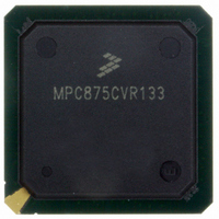
MPC875CVR133 Freescale Semiconductor, MPC875CVR133 Datasheet - Page 3

MPC875CVR133
Manufacturer Part Number
MPC875CVR133
Description
IC MPU POWERQUICC 133MHZ 256PBGA
Manufacturer
Freescale Semiconductor
Series
PowerQUICCr
Datasheet
1.MPC870VR80.pdf
(84 pages)
Specifications of MPC875CVR133
Processor Type
MPC8xx PowerQUICC 32-Bit
Speed
133MHz
Voltage
3.3V
Mounting Type
Surface Mount
Package / Case
256-PBGA
Processor Series
MPC8xx
Core
MPC8xx
Data Bus Width
32 bit
Maximum Clock Frequency
133 MHz
Operating Supply Voltage
0 V to 5 V
Maximum Operating Temperature
+ 100 C
Mounting Style
SMD/SMT
Data Ram Size
8 KB
I/o Voltage
5 V
Interface Type
I2C, SPI, UART
Minimum Operating Temperature
- 40 C
Program Memory Size
8 KB
Program Memory Type
EPROM/Flash
Core Size
32 Bit
Cpu Speed
133MHz
Digital Ic Case Style
BGA
No. Of Pins
256
Supply Voltage Range
1.7V To 1.9V
Rohs Compliant
Yes
Family Name
MPC8xx
Device Core
PowerQUICC
Device Core Size
32b
Frequency (max)
133MHz
Instruction Set Architecture
RISC
Supply Voltage 1 (typ)
1.8V
Operating Supply Voltage (max)
1.9V
Operating Supply Voltage (min)
1.7V
Operating Temp Range
-40C to 100C
Operating Temperature Classification
Industrial
Mounting
Surface Mount
Pin Count
256
Package Type
BGA
Lead Free Status / RoHS Status
Lead free / RoHS Compliant
Features
-
Lead Free Status / Rohs Status
Lead free / RoHS Compliant
Available stocks
Company
Part Number
Manufacturer
Quantity
Price
Company:
Part Number:
MPC875CVR133
Manufacturer:
Freescale Semiconductor
Quantity:
135
Company:
Part Number:
MPC875CVR133
Manufacturer:
Freescale Semiconductor
Quantity:
10 000
Freescale Semiconductor
•
•
•
•
•
•
Thirty-two address lines
Memory controller (eight banks)
— Contains complete dynamic RAM (DRAM) controller
— Each bank can be a chip select or RAS to support a DRAM bank
— Up to 30 wait states programmable per memory bank
— Glueless interface to DRAM, SIMMS, SRAM, EPROMs, Flash EPROMs, and other memory
— DRAM controller programmable to support most size and speed memory interfaces
— Four CAS lines, four WE lines, and one OE line
— Boot chip-select available at reset (options for 8-, 16-, or 32-bit memory)
— Variable block sizes (32 Kbytes–256 Mbytes)
— Selectable write protection
— On-chip bus arbitration logic
General-purpose timers
— Four 16-bit timers or two 32-bit timers
— Gate mode can enable/disable counting
— Interrupt can be masked on reference match and event capture
Two Fast Ethernet controllers (FEC)—Two 10/100 Mbps Ethernet/IEEE Std. 802.3® CDMA/CS
that interface through MII and/or RMII interfaces
System integration unit (SIU)
— Bus monitor
— Software watchdog
— Periodic interrupt timer (PIT)
— Clock synthesizer
— Decrementer and time base
— Reset controller
— IEEE 1149.1™ Std. test access port (JTAG)
Security engine is optimized to handle all the algorithms associated with IPsec, SSL/TLS, SRTP,
IEEE 802.11i® standard, and iSCSI processing. Available on the MPC875, the security engine
contains a crypto-channel, a controller, and a set of crypto hardware accelerators (CHAs). The
CHAs are:
— Data encryption standard execution unit (DEU)
— Advanced encryption standard unit (AESU)
devices
– DES, 3DES
– Two key (K1, K2, K1) or three key (K1, K2, K3)
– ECB and CBC modes for both DES and 3DES
– Implements the Rijndael symmetric key cipher
MPC875/MPC870 PowerQUICC™ Hardware Specifications, Rev. 4
Features
3


