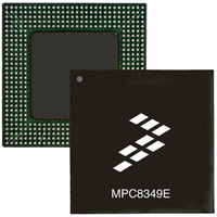
MPC8349VVAGDB Freescale Semiconductor, MPC8349VVAGDB Datasheet - Page 53

MPC8349VVAGDB
Manufacturer Part Number
MPC8349VVAGDB
Description
IC MPU POWERQUICC II 672-TBGA
Manufacturer
Freescale Semiconductor
Datasheet
1.MPC8349VVAGDB.pdf
(87 pages)
Specifications of MPC8349VVAGDB
Processor Type
MPC83xx PowerQUICC II Pro 32-Bit
Speed
400MHz
Voltage
1.2V
Mounting Type
Surface Mount
Package / Case
672-TBGA
Processor Series
MPC8xxx
Core
e300
Data Bus Width
32 bit
Development Tools By Supplier
MPC8349E-MITXE
Maximum Clock Frequency
400 MHz
Maximum Operating Temperature
+ 105 C
Mounting Style
SMD/SMT
I/o Voltage
1.8 V, 2.5 V, 3.3 V
Minimum Operating Temperature
0 C
Family Name
MPC83xx
Device Core
PowerQUICC II Pro
Device Core Size
32b
Frequency (max)
400MHz
Instruction Set Architecture
RISC
Supply Voltage 1 (typ)
1.2V
Operating Supply Voltage (max)
1.26V
Operating Supply Voltage (min)
1.14V
Operating Temp Range
0C to 105C
Operating Temperature Classification
Commercial
Mounting
Surface Mount
Pin Count
672
Package Type
TBGA
For Use With
MPC8349E-MITX-GP - KIT REFERENCE PLATFORM MPC8349EMPC8349E-MITXE - BOARD REFERENCE FOR MPC8349MPC8349EA-MDS-PB - KIT MODULAR DEV SYSTEM MPC8349E
Lead Free Status / RoHS Status
Lead free / RoHS Compliant
Features
-
Lead Free Status / Rohs Status
Lead free / RoHS Compliant
Available stocks
Company
Part Number
Manufacturer
Quantity
Price
Company:
Part Number:
MPC8349VVAGDB
Manufacturer:
Freescale Semiconductor
Quantity:
135
Company:
Part Number:
MPC8349VVAGDB
Manufacturer:
Freescale Semiconductor
Quantity:
10 000
Figure 36
Figure 37
generally reference the rising edge of the clock, these AC timing diagrams also apply when the falling edge
is the active edge.
Figure 37
Figure 38
18 Package and Pin Listings
This section details package parameters, pin assignments, and dimensions. The MPC8349EA is available
in a tape ball grid array (TBGA). See
Section 18.2, “Mechanical Dimensions for the MPC8349EA
Freescale Semiconductor
Note: The clock edge is selectable on SPI.
Note: The clock edge is selectable on SPI.
SPICLK (Output)
provides the AC test load for the SPI.
and
shows the SPI timings in slave mode (external clock).
Output Signals:
shows the SPI timings in master mode (internal clock).
SPICLK (Input)
Output Signals:
MPC8349EA PowerQUICC II Pro Integrated Host Processor Hardware Specifications, Rev. 12
Input Signals:
Input Signals:
(See Note)
(See Note)
Figure 38
(See Note)
(See Note)
SPIMOSI
SPIMISO
SPIMISO
SPIMOSI
Figure 38. SPI AC Timing in Master Mode (Internal Clock) Diagram
Figure 37. SPI AC Timing in Slave Mode (External Clock) Diagram
Output
represent the AC timings from
t
NEIVKH
t
NIIVKH
Section 18.1, “Package Parameters for the MPC8349EA TBGA”
Figure 36. SPI AC Test Load
Z
0
= 50 Ω
t
NIKHOX
t
NIIXKH
t
NEKHOX
t
NEIXKH
Table
TBGA.
54. Note that although the specifications
R
L
= 50 Ω
OV
DD
/2
Package and Pin Listings
and
53


