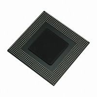
MPC8360EZUAJDGA Freescale Semiconductor, MPC8360EZUAJDGA Datasheet - Page 32

MPC8360EZUAJDGA
Manufacturer Part Number
MPC8360EZUAJDGA
Description
IC MPU POWERQUICC II PRO 740TBGA
Manufacturer
Freescale Semiconductor
Datasheet
1.MPC8360CZUAJDG.pdf
(108 pages)
Specifications of MPC8360EZUAJDGA
Processor Type
MPC83xx PowerQUICC II Pro 32-Bit
Speed
533MHz
Voltage
1.2V
Mounting Type
Surface Mount
Package / Case
740-TBGA
Processor Series
MPC8xxx
Core
e300
Data Bus Width
32 bit
Development Tools By Supplier
MPC8360E-RDK
Maximum Clock Frequency
533 MHz
Maximum Operating Temperature
+ 105 C
Mounting Style
SMD/SMT
I/o Voltage
1.8 V, 2.5 V, 3.3 V
Minimum Operating Temperature
0 C
For Use With
MPC8360EA-MDS-PB - KIT APPLICATION DEV 8360 SYSTEMMPC8360E-RDK - BOARD REFERENCE DESIGN FOR MPC
Lead Free Status / RoHS Status
Lead free / RoHS Compliant
Features
-
Lead Free Status / Rohs Status
Lead free / RoHS Compliant
Available stocks
Company
Part Number
Manufacturer
Quantity
Price
Company:
Part Number:
MPC8360EZUAJDGA
Manufacturer:
Freescale Semiconductor
Quantity:
10 000
UCC Ethernet Controller: Three-Speed Ethernet, MII Management
Figure 12
8.2.2.2
Table 30
32
At recommended operating conditions with LV
At recommended operating conditions with LV
TX_CLK data clock rise time, (20% to 80%)
TX_CLK data clock fall time, (80% to 20%)
Note:
1. The symbols used for timing specifications follow the pattern of t
RX_CLK clock period 10 Mbps
RX_CLK clock period 100 Mbps
RX_CLK duty cycle
RXD[3:0], RX_DV, RX_ER setup time to RX_CLK
RXD[3:0], RX_DV, RX_ER hold time to RX_CLK
RX_CLK clock rise time, (20% to 80%)
inputs and t
timing (MT) for the time t
the clock reference symbol representation is based on two to three letters representing the clock of a particular functional.
For example, the subscript of t
used with the appropriate letter: R (rise) or F (fall).
MPC8360E/MPC8358E PowerQUICC II Pro Processor Revision 2.x TBGA Silicon Hardware Specifications, Rev. 4
provides the MII receive AC timing specifications.
shows the MII transmit AC timing diagram.
(first two letters of functional block)(reference)(state)(signal)(state)
MII Receive AC Timing Specifications
TXD[3:0]
TX_CLK
TX_EN
TX_ER
Parameter/Condition
Parameter/Condition
Table 29. MII Transmit AC Timing Specifications (continued)
MTX
clock reference (K) going high (H) until data outputs (D) are invalid (X). Note that, in general,
MTX
Table 30. MII Receive AC Timing Specifications
Figure 12. MII Transmit AC Timing Diagram
represents the MII(M) transmit (TX) clock. For rise and fall times, the latter convention is
t
MTXH
DD
DD
/OV
/OV
t
DD
DD
MTX
of 3.3 V ± 10%.
of 3.3 V ± 10%.
t
MTKHDX
t
MTXF
t
(first two letters of functional block)(signal)(state)(reference)(state)
MRXH
Symbol
for outputs. For example, t
Symbol
t
t
MRDXKH
MRDVKH
t
t
t
t
t
MRXR
MTXR
MTXF
MRX
MRX
/t
MRX
1
1
t
MTXR
10.0
10.0
Min
Min
1.0
1.0
1.0
35
—
—
MTKHDX
Typ
Typ
400
40
—
—
—
—
—
—
Freescale Semiconductor
symbolizes MII transmit
Max
Max
4.0
4.0
4.0
65
—
—
—
—
Unit
Unit
for
ns
ns
ns
ns
ns
ns
ns
%


