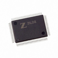
Z8018010FEC Zilog, Z8018010FEC Datasheet - Page 71

Z8018010FEC
Manufacturer Part Number
Z8018010FEC
Description
IC Z180 MPU 80QFP
Manufacturer
Zilog
Datasheet
1.Z8018006PSG.pdf
(85 pages)
Specifications of Z8018010FEC
Processor Type
Z180
Speed
10MHz
Voltage
5V
Mounting Type
Surface Mount
Package / Case
80-QFP
Processor Series
Z8018xx
Core
Z80
Data Bus Width
8 bit
Maximum Clock Frequency
10 MHz
Number Of Timers
2 bit
Operating Supply Voltage
0 V to 5 V
Maximum Operating Temperature
+ 100 C
Mounting Style
SMD/SMT
Minimum Operating Temperature
- 40 C
Height
2.8 mm
Length
20 mm
Supply Voltage (max)
5.5 V
Supply Voltage (min)
4.5 V
Width
14 mm
Lead Free Status / RoHS Status
Contains lead / RoHS non-compliant
Features
-
Lead Free Status / Rohs Status
No RoHS Version Available
Available stocks
Company
Part Number
Manufacturer
Quantity
Price
DMA/WAIT Control Register (DCNTL)
DMA/WAIT Control Register (DCNTL: I/O Address = 32h)
PS014004-1106
Bit
MMOD: Memory Mode Channel 0 (bit 1). When channel 0 is configured for memory
to/from memory transfers there is no
timing. Instead, two automatic transfer timing modes are selectable: burst (
cycle steal (
control of the bus continuously until the DMA transfer completes (the byte count register is
0
until the transfer is completed.
For channel 0 DMA with I/O source or destination, the selected
signal times the transfer and
DCNTL
I/O. DCNTL also defines the Request signal for each channel as level or edge sense.
also sets the DMA transfer mode for channel 1, which is limited to memory to/from I/O
transfers.
MWI1, MWI0: Memory Wait Insertion (bits 7-6)—Specifies the number of wait states
introduced into CPU or DMAC memory access cycles.
RESET
IWI1, IWI0: I/O Wait Insertion (bits 5-4)—Specifies the number of wait states
introduced into CPU or DMAC I/O access cycles.
DMS1, DMS0: DMA Request Sense (bits 3-2)—
request sense for channel 0 and channel 1 respectively. When reset to
sense. When set to
RESET
Typically, for an input/source device, the associated DMS bit must be
programmed as
update its
machine cycles involved in transferring a byte.
An output/destination device takes much less time to update its
DMA channel starts a
). In
MWI1
R/W
Figure 67. DMA/WAIT Control Register (DCNTL: I/O Address = 32h
7
CYCLE STEAL
.
.
controls the insertion of wait states into DMAC (and CPU) accesses of memory or
MWI0
R/W
REQUEST
6
MMOD = 0
0
for level sense because the device undertakes a relatively long period to
IWI1
R/W
1
5
, the input is edge sense.
signal after the DMA channel reads data from it in the first of the two
mode, the CPU is provided a cycle for each DMA byte transfer cycle
WRITE
). For burst memory to/from memory transfers, the DMAC takes
R/W
IWI0
4
MMOD
operation to it, as the
DMS1
R/W
3
is ignored.
REQUEST HANDSHAKE
DMS0
R/W
2
DMS1
MMOD
IWI1
DIM1
R/W
and
1
DMS1
MWI1
is cleared to
and
DMS0
DIM0
R/W
IWI0
0
and
and
signal to control the transfer
are cleared to
REQUEST
REQUEST HANDSHAKE
are set to
DMS0
MWI0
Microprocessor Unit
0
0
during
, the input is level
specify the DMA
are set to
signal, after the
MMOD = 1
1
during
0
RESET
during
Architecture
1
Z80180
DCNTL
.
RESET
during
) and
.
65


