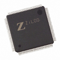
Z84C9008ASG Zilog, Z84C9008ASG Datasheet - Page 13

Z84C9008ASG
Manufacturer Part Number
Z84C9008ASG
Description
OC 8MHZ Z80 KIO 100 LQFP
Manufacturer
Zilog
Datasheet
1.Z84C9010VEG.pdf
(31 pages)
Specifications of Z84C9008ASG
Processor Type
Z80
Features
Serial/Parallel Input/Output, Counter/Timer Circuit
Speed
8MHz
Voltage
5V
Mounting Type
Surface Mount
Package / Case
100-LQFP
Lead Free Status / RoHS Status
Lead free / RoHS Compliant
Available stocks
Company
Part Number
Manufacturer
Quantity
Price
PS011802-0902
•
•
All control registers must be rewritten after a hardware reset.
RTSA, RTSB. Request to Send (outputs, Active Low). These signals are modem control
signals for their serial channels. They follow the inverse state programmed into their
respective serial channels, and are multiplexed with Port C, bits 4 and 3, respectively.
RxCA, RxCB. Receive Clock (inputs, Active Low). These clocks are used to assemble
the data in the receiver shift register for their serial channels. Data is sampled on the rising
edge of the clock.
RxDA, RxDB. Receive Data (inputs, Active High). These pins are the input data pins to
the receive shift register for their serial channels.
SYNCA, SYNCB. Synchronization (bidirectional, Active Low). In the Asynchronous
mode of operation, these pins act much like the CTS and DCD pins. Transitions affect the
Sync/Hunt status bit for their respective serial channels, but serve no other purpose. These
pins are multiplexed with Port C, bits 6 and 1, respectively.
TxCA, TxCB. Transmit Clock (inputs, Active Low). These clocks are used to transmit
data from the transmit shift register for their serial channels. Data is transmitted on the
falling edge of the clock.
TxDA, TxDB. Transmit Data (outputs, Active High). These pins are the output data pins
from the transmitter for their serial channels.
WT/RDYA, WT/RDYB. Wait/Ready (outputs, open-drain when programmed as Wait;
tristated when programmed as Ready). These pins may be programmed as Ready lines for
a DMA controller or Wait lines for interfacing to a CPU. As a Ready line, these pins indi-
cate (when Active Low) that the transmitter or the receiver requests a transfer between the
serial channel and the DMA. As a Wait line, these pins dictate (when Low) that the CPU
must wait until the transmitter or receiver can complete the requested transaction. These
pins are multiplexed with Port C, bit 7 and 0, respectively.
XTALI. Crystal/Clock Connection. (input).
XTALO. Crystal Connection. (output).
ZC/TO0–ZC/TO3. Zero count/Time-out (outputs, Active High). These four pins are out-
puts from the four counter/timer channels of the KIO. Each pin pulses High when its cor-
responding downcounter reaches 0.
SIO channels disabled
Marking with interrupts disabled.
KIO Serial/Parallel Counter Timer
Z84C90
8


