MPC8323CVRADDC Freescale Semiconductor, MPC8323CVRADDC Datasheet - Page 42
MPC8323CVRADDC
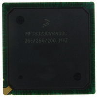
Manufacturer Part Number
MPC8323CVRADDC
Description
IC MPU PWRQUICC II 516-PBGA
Manufacturer
Freescale Semiconductor
Datasheet
1.MPC8321VRADDC.pdf
(82 pages)
Specifications of MPC8323CVRADDC
Processor Type
MPC83xx PowerQUICC II Pro 32-Bit
Speed
266MHz
Voltage
1V
Mounting Type
Surface Mount
Package / Case
516-PBGA
For Use With
MPC8323E-RDB - BOARD REFERENCE DESIGN
Lead Free Status / RoHS Status
Lead free / RoHS Compliant
Features
-
Available stocks
Company
Part Number
Manufacturer
Quantity
Price
Company:

Part Number:
MPC8323CVRADDC
Manufacturer:
Freescale Semiconductor
Quantity:
10 000


TDM/SI
17.2
Table 47
Figure 33
Figure 34
reference the rising edge of the clock, these AC timing diagrams also apply when the falling edge is the
active edge.
42
Input low voltage
Input current
TDM/SI outputs—External clock delay
TDM/SI outputs—External clock High Impedance
TDM/SI inputs—External clock input setup time
TDM/SI inputs—External clock input hold time
Notes:
1. Output specifications are measured from the 50% level of the rising edge of CLKIN to the 50% level of the signal. Timings
2. The symbols used for timing specifications follow the pattern of t
are measured at the pin.
inputs and t
outputs external timing (SE) for the time t
are invalid (X).
MPC8323E PowerQUICC II Pro Integrated Communications Processor Family Hardware Specifications, Rev. 4
TDM/SICLK (Input)
provides the TDM/SI input and output AC timing specifications.
Note: The clock edge is selectable on TDM/SI.
TDM/SI AC Timing Specifications
provides the AC test load for the TDM/SI.
represents the AC timing from
Output Signals:
(first two letters of functional block)(reference)(state)(signal)(state)
Characteristic
Input Signals:
(See Note)
(See Note)
TDM/SI
TDM/SI
Characteristic
Output
Table 46. TDM/SI DC Electrical Characteristics (continued)
Figure 34. TDM/SI AC Timing (External Clock) Diagram
t
SEIVKH
Table 47. TDM/SI AC Timing Specifications
TDM/SI
Figure 33. TDM/SI AC Test Load
Z
Table
Symbol
0
memory clock reference (K) goes from the high state (H) until outputs (O)
= 50 Ω
V
I
IN
IL
t
SEKHOX
47. Note that although the specifications generally
t
SEKHOV
0 V ≤ V
t
SEIXKH
Condition
(first two letters of functional block)(signal)(state)(reference)(state)
for outputs. For example, t
IN
—
≤ OV
Symbol
t
t
t
t
SEKHOV
SEKHOX
SEIVKH
SEIXKH
R
L
DD
= 50 Ω
2
1
–0.3
Min
—
OV
Min
2
2
5
2
DD
SEKHOX
/2
Freescale Semiconductor
symbolizes the TDM/SI
Max
0.8
±5
Max
12
10
—
—
Unit
Unit
μA
ns
ns
ns
ns
for
V
Related parts for MPC8323CVRADDC
Image
Part Number
Description
Manufacturer
Datasheet
Request
R

Part Number:
Description:
Manufacturer:
Freescale Semiconductor, Inc
Datasheet:
Part Number:
Description:
Manufacturer:
Freescale Semiconductor, Inc
Datasheet:
Part Number:
Description:
Manufacturer:
Freescale Semiconductor, Inc
Datasheet:
Part Number:
Description:
Manufacturer:
Freescale Semiconductor, Inc
Datasheet:
Part Number:
Description:
Manufacturer:
Freescale Semiconductor, Inc
Datasheet:
Part Number:
Description:
Manufacturer:
Freescale Semiconductor, Inc
Datasheet:
Part Number:
Description:
Manufacturer:
Freescale Semiconductor, Inc
Datasheet:
Part Number:
Description:
Manufacturer:
Freescale Semiconductor, Inc
Datasheet:
Part Number:
Description:
Manufacturer:
Freescale Semiconductor, Inc
Datasheet:
Part Number:
Description:
Manufacturer:
Freescale Semiconductor, Inc
Datasheet:
Part Number:
Description:
Manufacturer:
Freescale Semiconductor, Inc
Datasheet:
Part Number:
Description:
Manufacturer:
Freescale Semiconductor, Inc
Datasheet:
Part Number:
Description:
Manufacturer:
Freescale Semiconductor, Inc
Datasheet:
Part Number:
Description:
Manufacturer:
Freescale Semiconductor, Inc
Datasheet:
Part Number:
Description:
Manufacturer:
Freescale Semiconductor, Inc
Datasheet: