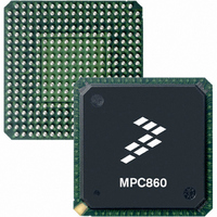
MPC8241LZQ266D Freescale Semiconductor, MPC8241LZQ266D Datasheet - Page 40

MPC8241LZQ266D
Manufacturer Part Number
MPC8241LZQ266D
Description
IC MPU 32BIT 266MHZ 357-PBGA
Manufacturer
Freescale Semiconductor
Datasheet
1.MPC8241LZQ200D.pdf
(58 pages)
Specifications of MPC8241LZQ266D
Processor Type
MPC82xx PowerQUICC II 32-bit
Speed
266MHz
Voltage
1.8V
Mounting Type
Surface Mount
Package / Case
357-PBGA
Lead Free Status / RoHS Status
Contains lead / RoHS non-compliant
Features
-
Available stocks
Company
Part Number
Manufacturer
Quantity
Price
Company:
Part Number:
MPC8241LZQ266D
Manufacturer:
ON
Quantity:
102
Company:
Part Number:
MPC8241LZQ266D
Manufacturer:
Freescale Semiconductor
Quantity:
10 000
PLL Configuration
40
Notes:
1. PLL_CFG[0:4] settings not listed are reserved. Bits 7–4 of register offset <0xE2> contain the PLL_CFG[0:4] setting value.
2. Range values are shown rounded down to the nearest whole number (decimal place accuracy removed) for clarity.
3. Limited by maximum PCI input frequency (66 MHz).
4. Limited by minimum CPU VCO frequency (300 MHz).
5. Limited by maximum CPU operating frequency.
6. In PLL bypass mode, the PCI_SYNC_IN input signal clocks the internal processor directly, the peripheral logic PLL is
7. Limited by minimum CPU operating frequency (100 MHz).
8. Limited due to maximum memory VCO frequency (352 MHz).
9. In dual PLL bypass mode, the PCI_SYNC_IN input signal clocks the internal peripheral logic directly, the peripheral logic PLL
10.Limited by maximum CPU VCO frequency (704 MHz).
11.Limited by maximum system memory interface operating frequency (83 MHz @ 166 MHz CPU bus speed).
12.Limited by maximum system memory interface operating frequency (100 MHz @ 200 MHz CPU bus speed).
13.Limited by minimum memory VCO frequency (132 MHz).
14.In clock off mode, no clocking occurs inside the MPC8241, regardless of the PCI_SYNC_IN input.
Ref
1E
1F
Note the impact of the relevant revisions for mode 7.
disabled, and the bus mode is set for 1:1 (PCI:Mem) mode operation. This mode is intended for hardware modeling. The
AC timing specifications in this document do not apply in PLL bypass mode.
is disabled, and the bus mode is set for 1:1 (PCI_SYNC_IN:Mem) mode operation. In this mode, the OSC_IN input signal
clocks the internal processor directly in 1:1 (OSC_IN:CPU) mode operation, and the processor PLL is disabled. The
PCI_SYNC_IN and OSC_IN input clocks must be externally synchronized. This mode is intended for hardware modeling.
The AC timing specifications in this document do not apply in dual PLL bypass mode.
Ref
0
1
2
3
4
2
2
PLL_CFG
11110
11111
[0:4]
CFG[0:4]
14
14
1
00011
00000
00001
00010
00100
PLL_
PCI Clock
SYNC_IN)
Range
12
10,11
(MHz)
Input
(PCI_
Table 17. PLL Configurations (166- and 200-MHz) (continued)
MPC8241 Integrated Processor Hardware Specifications, Rev. 10
3
166 MHz-Part
PCI Clock Input
(PCI_SYNC_IN)
Table 18. PLL Configurations (266-MHz Parts)
Not usable
Not usable
Peripheral
Bus Clock
50
50
Range
Logic/
Range
(MHz)
25–35
25–29
25–44
Mem
(MHz)
15
14
–59
–66
5
5
4
1
5
1
2
Range
Clock
(MHz)
CPU
266-MHz Part
Periph Logic/
Clock Range
Mem Bus
75–105
(MHz)
75–88
50–59
50–66
50–88
PCI Clock
SYNC_IN)
Range
(MHz)
Input
(PCI_
9
3
200-MHz Part
Peripheral
Not usable
Not usable
Mem Bus
Range
Logic/
Clock
(MHz)
CPU Clock
188–263
225–264
225–266
100–133
100–176
Range
(MHz)
2
Range
Clock
(MHz)
CPU
PCI-to-Mem
(Mem VCO)
1 (Bypass)
3 (2)
3 (2)
1 (4)
2 (4)
(Mem VCO)
Freescale Semiconductor
PCI-to-
Mem
Multipliers
Off
Off
Multipliers
Mem-to-CPU
(CPU VCO)
(CPU VCO)
2.5 (2)
4.5 (2)
Mem-to-
3 (2)
2 (4)
2 (4)
CPU
Off
Off


