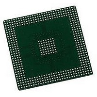
MPC5200CBV400 Freescale Semiconductor, MPC5200CBV400 Datasheet - Page 72

MPC5200CBV400
Manufacturer Part Number
MPC5200CBV400
Description
IC MPU 32BIT 400MHZ PPC 272-PBGA
Manufacturer
Freescale Semiconductor
Datasheet
1.MPC5200CVR400B.pdf
(80 pages)
Specifications of MPC5200CBV400
Processor Type
MPC52xx PowerPC 32-Bit
Speed
400MHz
Voltage
1.5V
Mounting Type
Surface Mount
Package / Case
272-PBGA
Core Size
32 Bit
No. Of I/o's
56
Ram Memory Size
16KB
Cpu Speed
400MHz
No. Of Timers
8
Embedded Interface Type
CAN, I2C, SPI, UART, USB
No. Of Pwm Channels
8
Digital Ic Case Style
BGA
Rohs Compliant
No
Family Name
MPC52xx
Device Core
PowerPC
Device Core Size
32b
Frequency (max)
400MHz
Instruction Set Architecture
RISC
Supply Voltage 1 (typ)
1.5V
Operating Supply Voltage (max)
1.58V
Operating Supply Voltage (min)
1.42V
Operating Temp Range
-40C to 85C
Operating Temperature Classification
Industrial
Mounting
Surface Mount
Pin Count
272
Package Type
BGA
Lead Free Status / RoHS Status
Contains lead / RoHS non-compliant
Features
-
Lead Free Status / Rohs Status
Not Compliant
Available stocks
Company
Part Number
Manufacturer
Quantity
Price
Company:
Part Number:
MPC5200CBV400
Manufacturer:
FREESCAL
Quantity:
200
Company:
Part Number:
MPC5200CBV400
Manufacturer:
Freescale Semiconductor
Quantity:
10 000
Company:
Part Number:
MPC5200CBV400B
Manufacturer:
FREESCAL
Quantity:
200
System Design Information
The relationship between VDD_IO_MEM and VDD_IO is non-critical during power-up and power-down
sequences. Both VDD_IO_MEM (2.5 V or 3.3 V) and VDD_IO are specified relative to VDD_CORE.
5.1.1
If VDD_IO/VDD_IO_MEM are powered up with the VDD_CORE at 0V, the sense circuits in the I/O pads
will cause all pad output drivers connected to the VDD_IO/VDD_IO_MEM to be in a high-impedance
state. There is no limit to how long after VDD_IO/VDD_IO_MEM powers up before VDD_CORE must
power up. VDD_CORE should not lead the VDD_IO, VDD_IO_MEM or PLL_AVDD by more than 0.4
V during power ramp up or there will be high current in the internal ESD protection diodes. The rise times
on the power supplies should be slower than 1 microsecond to avoid turning on the internal ESD protection
clamp diodes.
The recommended power up sequence is as follows:
Use one microsecond or slower rise time for all supplies.
72
Note:
1. VDD_CORE should not exceed VDD_IO, VDD_IO_MEM or PLL_AVDD by more than
2. It is recommended that VDD_CORE/PLL_AVDD should track VDD_IO/VDD_IO_MEM
3. Input voltage must not be greater than the supply voltage (VDD_IO, VDD_IO_MEM,
4. Use 1 microsecond or slower rise time for all supplies.
3.3V
2.5V
1.5V
0
0.4 V at any time, including power-up.
up to 0.9 V then separate for completion of ramps.
VDD_CORE, or PLL_AVDD) by more than 0.5 V at any time, including during power-up.
Power Up Sequence
1
2
Figure 52. Supply Voltage Sequencing
MPC5200 Data Sheet, Rev. 4
VDD_IO,
VDD_IO_MEM (SDR)
VDD_IO_MEM (DDR)
VDD_CORE,
PLL_AVDD
Freescale Semiconductor
Time


