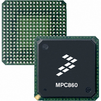
MPC866PCZP100A Freescale Semiconductor, MPC866PCZP100A Datasheet - Page 3

MPC866PCZP100A
Manufacturer Part Number
MPC866PCZP100A
Description
IC MPU POWERQUICC 100MHZ 357PBGA
Manufacturer
Freescale Semiconductor
Datasheet
1.MPC859DSLCVR50A.pdf
(96 pages)
Specifications of MPC866PCZP100A
Processor Type
MPC8xx PowerQUICC 32-Bit
Speed
100MHz
Voltage
1.8V
Mounting Type
Surface Mount
Package / Case
357-PBGA
Lead Free Status / RoHS Status
Contains lead / RoHS non-compliant
Features
-
Available stocks
Company
Part Number
Manufacturer
Quantity
Price
Company:
Part Number:
MPC866PCZP100A
Manufacturer:
MPC
Quantity:
648
Company:
Part Number:
MPC866PCZP100A
Manufacturer:
Freescale Semiconductor
Quantity:
10 000
Freescale Semiconductor
•
•
•
•
•
•
— ATM port-to-port switching capability without the need for RAM-based microcode
— Simultaneous MII (10/100Base-T) and UTOPIA (half-duplex) capability
— Optional statistical cell counters per PHY
— UTOPIA level 2 compliant interface with added FIFO buffering to reduce the total cell transmission
— Parameter RAM for both SPI and I
— Supports full-duplex UTOPIA both master (ATM side) and slave (PHY side) operation using a 'split' bus
— AAL2/VBR functionality is ROM-resident.
Up to 32-bit data bus (dynamic bus sizing for 8, 16, and 32 bits)
Thirty-two address lines
Memory controller (eight banks)
— Contains complete dynamic RAM (DRAM) controller
— Each bank can be a chip select or RAS to support a DRAM bank
— Up to 30 wait states programmable per memory bank
— Glueless interface to page mode/EDO/SDRAM, SRAM, EPROMs, flash EPROMs, and other memory
— DRAM controller programmable to support most size and speed memory interfaces
— Four CAS lines, four WE lines, and one OE line
— Boot chip-select available at reset (options for 8-, 16-, or 32-bit memory)
— Variable block sizes (32 Kbytes–256 Mbytes)
— Selectable write protection
— On-chip bus arbitration logic
General-purpose timers
— Four 16-bit timers cascadable to be two 32-bit timers
— Gate mode can enable/disable counting
— Interrupt can be masked on reference match and event capture
Fast Ethernet controller (FEC)
— Simultaneous MII (10/100Base-T) and UTOPIA operation when using the UTOPIA multiplexed bus
System integration unit (SIU)
— Bus monitor
— Software watchdog
— Periodic interrupt timer (PIT)
— Low-power stop mode
— Clock synthesizer
— Decrementer and time base from the PowerPC architecture
— Reset controller
— IEEE 1149.1 test access port (JTAG)
time. (The earlier UTOPIA level 1 specification is also supported.)
– Multi-PHY support on the MPC866, MPC859P, and MPC859T
– Four PHY support on the MPC866/859
devices.
MPC866/MPC859 Hardware Specifications, Rev. 2
2
C can be relocated without RAM-based microcode
Features
3


