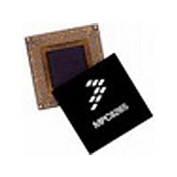
MPC8255ACZUMHBB Freescale Semiconductor, MPC8255ACZUMHBB Datasheet - Page 17

MPC8255ACZUMHBB
Manufacturer Part Number
MPC8255ACZUMHBB
Description
IC MPU POWERQUICC II 480-TBGA
Manufacturer
Freescale Semiconductor
Specifications of MPC8255ACZUMHBB
Processor Type
MPC82xx PowerQUICC II 32-bit
Speed
266MHz
Voltage
2V
Mounting Type
Surface Mount
Package / Case
480-TBGA
Family Name
MPC82XX
Device Core
PowerQUICC II
Device Core Size
32b
Frequency (max)
266MHz
Instruction Set Architecture
RISC
Supply Voltage 1 (typ)
2V
Operating Supply Voltage (max)
2.1V
Operating Supply Voltage (min)
1.9V
Operating Temp Range
-40C to 105C
Operating Temperature Classification
Industrial
Mounting
Surface Mount
Pin Count
480
Package Type
TBGA
Lead Free Status / RoHS Status
Contains lead / RoHS non-compliant
Features
-
Lead Free Status / Rohs Status
Not Compliant
Available stocks
Company
Part Number
Manufacturer
Quantity
Price
Company:
Part Number:
MPC8255ACZUMHBB
Manufacturer:
MOTOROLA
Quantity:
745
Company:
Part Number:
MPC8255ACZUMHBB
Manufacturer:
Freescale Semiconductor
Quantity:
10 000
Part Number:
MPC8255ACZUMHBB
Manufacturer:
FREESCALE
Quantity:
20 000
1
Table 10
Figure 8
Freescale Semiconductor
Note:
Output specifications are measured from the 50% level of the rising edge of CLKIN to the 50% level of the signal. Timings are
measured at the pin.
sp33a
sp33b
sp31
sp32
sp34
sp35
Max
Spec Number
shows TDM input and output signals.
lists SIU output characteristics.
MPC8260 PowerQUICC II Integrated Communications Processor Hardware Specifications, Rev. 2
sp30
sp30
sp30
sp30
sp30
sp30
Min
Activating data pipelining (setting BRx[DR] in the memory controller)
improves the AC timing. When data pipelining is activated, sp12 can be
used for data bus setup even when ECC or PARITY are used. Also, sp33a
can be used as the AC specification for DP signals.
Note: There are four possible TDM timing conditions:
1. Input sampled on the rising edge and output driven on the rising edge (shown).
2. Input sampled on the rising edge and output driven on the falling edge.
3. Input sampled on the falling edge and output driven on the falling edge.
4. Input sampled on the falling edge and output driven on the rising edge.
PSDVAL/TEA/TA
ADD/ADD_atr./BADDR/CI/GBL/WT
Data bus
DP
memc signals/ALE
all other signals
TDM output signals
TDM input signals
Serial CLKin
Table 10. AC Characteristics for SIU Outputs
Figure 8. TDM Signal Diagram
Characteristic
NOTE
sp20
sp40/sp41
sp21
1
Electrical and Thermal Characteristics
Max Delay (ns)
66 MHz
7.5
10
12
8
8
6
Min Delay (ns)
66 MHz
0.5
0.5
0.5
0.5
0.5
0.5
17


