MPC8321ECZQAFDC Freescale Semiconductor, MPC8321ECZQAFDC Datasheet - Page 33
MPC8321ECZQAFDC
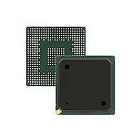
Manufacturer Part Number
MPC8321ECZQAFDC
Description
IC MPU PWRQUICC II 516-PBGA
Manufacturer
Freescale Semiconductor
Datasheet
1.MPC8321VRADDC.pdf
(82 pages)
Specifications of MPC8321ECZQAFDC
Processor Type
MPC83xx PowerQUICC II Pro 32-Bit
Speed
333MHz
Voltage
1V
Mounting Type
Surface Mount
Package / Case
516-PBGA
Processor Series
MPC8xxx
Core
e300
Data Bus Width
32 bit
Development Tools By Supplier
MPC8323E-MDS-PB
Maximum Clock Frequency
333 MHz
Maximum Operating Temperature
+ 105 C
Mounting Style
SMD/SMT
Data Ram Size
16 KB
I/o Voltage
1.8 V, 3.3 V
Interface Type
I2C, SPI, UART
Minimum Operating Temperature
- 40 C
Family Name
MPC83xx
Device Core
PowerQUICC II Pro
Device Core Size
32b
Frequency (max)
333MHz
Instruction Set Architecture
RISC
Supply Voltage 1 (typ)
1V
Operating Supply Voltage (max)
1.05V
Operating Supply Voltage (min)
0.95V
Operating Temp Range
-40C to 105C
Operating Temperature Classification
Industrial
Mounting
Surface Mount
Pin Count
516
Package Type
TEBGA
Lead Free Status / RoHS Status
Lead free / RoHS Compliant
Features
-
Lead Free Status / Rohs Status
Lead free / RoHS Compliant
Available stocks
Company
Part Number
Manufacturer
Quantity
Price
Company:

Part Number:
MPC8321ECZQAFDC
Manufacturer:
Freescale Semiconductor
Quantity:
10 000


11 I
This section describes the DC and AC electrical characteristics for the I
11.1
Table 33
11.2
Table 34
Freescale Semiconductor
At recommended operating conditions with OV
All values refer to V
Input high voltage level
Input low voltage level
Low level output voltage
Output fall time from V
capacitance from 10 to 400 pF
Pulse width of spikes which must be suppressed by the
input filter
Capacitance for each I/O pin
Input current (0 V ≤ V
Notes:
1. Output voltage (open drain or open collector) condition = 3 mA sink current.
2. C
3. Refer to the MPC8323E PowerQUICC II Pro Integrated Communications Processor Reference Manual for information on the
4. I/O pins obstructs the SDA and SCL lines if OV
SCL clock frequency
Low period of the SCL clock
High period of the SCL clock
Setup time for a repeated START condition
Hold time (repeated) START condition (after this period, the first clock
pulse is generated)
Data setup time
Data hold time:
digital filter used.
B
MPC8323E PowerQUICC II Pro Integrated Communications Processor Family Hardware Specifications, Rev. 4
= capacitance of one bus line in pF.
2
provides the DC electrical characteristics for the I
provides the AC timing parameters for the I
I
I
C
2
2
C DC Electrical Characteristics
C AC Electrical Specifications
IH
(min) and V
IN
IH
Parameter
≤ OV
(min) to V
DD
Parameter
IL
(max) levels (see
)
IL
(max) with a bus
Table 33. I
Table 34. I
DD
CBUS compatible masters
of 3.3 V ± 10%.
Table
DD
2
2
C DC Electrical Characteristics
C AC Electrical Specifications
33).
is switched off.
I
2
C bus devices
Symbol
t
t
I2KLKV
I2KHKL
V
V
V
I
2
C
IN
OL
IH
IL
C interface of the MPC8323E.
I
2
Symbol
C interface of the MPC8323E.
t
t
t
t
20 + 0.1 × C
I2SVKH
I2DVKH
I2SXKL
I2DXKL
t
t
0.7 × OV
I2CH
f
I2CL
I2C
–0.3
Min
—
—
0
0
1
DD
B
2
C interface of the MPC8323E.
Min
100
1.3
0.6
0.6
0.6
—
0
0
OV
0.3 × OV
2
DD
Max
250
0.4
50
10
±5
+ 0.3
DD
Max
0.9
400
—
—
—
—
—
—
Unit
3
μA
pF
ns
ns
V
V
V
Notes
Unit
kHz
μs
μs
μs
μs
ns
μs
—
—
—
1
2
3
4
I
33
2
C
Related parts for MPC8321ECZQAFDC
Image
Part Number
Description
Manufacturer
Datasheet
Request
R

Part Number:
Description:
Mpc8321e Powerquicc Ii Pro Processor
Manufacturer:
Freescale Semiconductor, Inc
Datasheet:
Part Number:
Description:
Manufacturer:
Freescale Semiconductor, Inc
Datasheet:
Part Number:
Description:
Manufacturer:
Freescale Semiconductor, Inc
Datasheet:
Part Number:
Description:
Manufacturer:
Freescale Semiconductor, Inc
Datasheet:
Part Number:
Description:
Manufacturer:
Freescale Semiconductor, Inc
Datasheet:
Part Number:
Description:
Manufacturer:
Freescale Semiconductor, Inc
Datasheet:
Part Number:
Description:
Manufacturer:
Freescale Semiconductor, Inc
Datasheet:
Part Number:
Description:
Manufacturer:
Freescale Semiconductor, Inc
Datasheet:
Part Number:
Description:
Manufacturer:
Freescale Semiconductor, Inc
Datasheet:
Part Number:
Description:
Manufacturer:
Freescale Semiconductor, Inc
Datasheet:
Part Number:
Description:
Manufacturer:
Freescale Semiconductor, Inc
Datasheet:
Part Number:
Description:
Manufacturer:
Freescale Semiconductor, Inc
Datasheet:
Part Number:
Description:
Manufacturer:
Freescale Semiconductor, Inc
Datasheet:
Part Number:
Description:
Manufacturer:
Freescale Semiconductor, Inc
Datasheet:
Part Number:
Description:
Manufacturer:
Freescale Semiconductor, Inc
Datasheet: