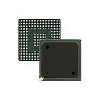
MPC8321CZQADDC Freescale Semiconductor, MPC8321CZQADDC Datasheet - Page 81

MPC8321CZQADDC
Manufacturer Part Number
MPC8321CZQADDC
Description
IC MPU PWRQUICC II 516-PBGA
Manufacturer
Freescale Semiconductor
Datasheet
1.MPC8321VRADDC.pdf
(82 pages)
Specifications of MPC8321CZQADDC
Processor Type
MPC83xx PowerQUICC II Pro 32-Bit
Speed
266MHz
Voltage
1V
Mounting Type
Surface Mount
Package / Case
516-PBGA
Processor Series
MPC8xxx
Core
e300
Data Bus Width
32 bit
Development Tools By Supplier
MPC8323E-MDS-PB
Maximum Clock Frequency
266 MHz
Maximum Operating Temperature
+ 105 C
Mounting Style
SMD/SMT
Data Ram Size
16 KB
I/o Voltage
1.8 V, 3.3 V
Interface Type
I2C, SPI, UART
Minimum Operating Temperature
- 40 C
Family Name
MPC83xx
Device Core
PowerQUICC II Pro
Device Core Size
32b
Frequency (max)
266MHz
Instruction Set Architecture
RISC
Supply Voltage 1 (typ)
1V
Operating Supply Voltage (max)
1.05V
Operating Supply Voltage (min)
0.95V
Operating Temp Range
-40C to 105C
Operating Temperature Classification
Industrial
Mounting
Surface Mount
Pin Count
516
Package Type
TEBGA
Lead Free Status / RoHS Status
Lead free / RoHS Compliant
Features
-
Lead Free Status / Rohs Status
Lead free / RoHS Compliant
Available stocks
Company
Part Number
Manufacturer
Quantity
Price
Company:
Part Number:
MPC8321CZQADDC
Manufacturer:
MOTOROLA
Quantity:
996
Company:
Part Number:
MPC8321CZQADDC
Manufacturer:
Freescale Semiconductor
Quantity:
10 000
Freescale Semiconductor
Rev.
No.
2
1
0
MPC8323E PowerQUICC II Pro Integrated Communications Processor Family Hardware Specifications, Rev. 4
4/2008
6/2007
6/2007
Date
Correction to descriptive text in Section 2.2.
Initial release.
• Removed Figures 2 and 3 overshoot and undershoot voltage specs from
• Corrected QUIESCE signal to be an output signal in
• Added column for GVDD (1.8 V) - DDR2 - to
• Added
• Removed CE_TRB* and CE_PIO* signals from
• Added three local bus AC specifications to
• Added row in
• Modified
Voltage
local bus clock).
Figure 4
Specification,” and footnotes 4 and 5 from
Section 2.2, “Power
Table 2
Table 67. Document Revision History
DDR input timing diagram.
stating junction temperature range of 0 to 105•C. C.
Sequencing,” to include PORESET requirement.
Substantive Change(s)
Table 30
Table 6
Table
Table
(duty cycle, jitter, delay between input clock and
Table
with 0.212-W typical power dissipation.
55.
1.
55.
Section 2.1.2, “Power Supply
Document Revision History
81


