CS42L52-CNZ Cirrus Logic Inc, CS42L52-CNZ Datasheet
CS42L52-CNZ
Specifications of CS42L52-CNZ
Available stocks


Related parts for CS42L52-CNZ


CS42L52-CNZ Summary of contents
Page 1
... Serial Audio 2 Reset I C Control Input/Output Copyright © Cirrus Logic, Inc. 2008 (All Rights Reserved) CS42L52 2 x 1.00 W into 8 Ω 550 mW into 8 Ω 230 mW into 8 Ω 1.90 W into 4 Ω 1.00 W into 4 Ω 350 mW into 4 Ω @ 2.5 V Battery Level Monitoring & Compensation ...
Page 2
... The CS42L52 is available in a 40-pin QFN package in both Commercial (-40 to +85 °C) and Automotive (-40 to +105 °C) grades. The CS42L52 Customer Demonstration board is also available for device evaluation and implementation sugges- tions ...
Page 3
... Mono Speaker Output Configuration ..................................................................................... 33 4.5.2 VP Battery Compensation ..................................................................................................... 33 4.5.2.1 Maintaining a Desired Output Level ........................................................................... 34 4.6 Serial Port Clocking ........................................................................................................................ 34 4.7 Digital Interface Formats ................................................................................................................ 36 4.7.1 DSP Mode ............................................................................................................................. 36 4.8 Initialization ..................................................................................................................................... 37 4.9 Recommended Power-up Sequence .............................................................................................. 37 4.10 Recommended Power-down Sequence ....................................................................................... 37 4.11 Required Initialization Settings ..................................................................................................... 37 4.12 Control Port Operation .................................................................................................................. 38 DS680F1 5/13/08 CS42L52 3 ...
Page 4
... Ch. x Analog Soft Ramp ........................................................................................................ 49 6.9.4 Ch. x Analog Zero Cross ....................................................................................................... 49 6.10 ADC HPF Corner Frequency (Address 0Bh) ................................................................................ 50 6.10.1 HPF x Corner Frequency .................................................................................................... 50 6.11 Misc. ADC Control (Address 0Ch) ................................................................................................ 50 6.11.1 Analog Front-End Volume Setting B=A ............................................................................... 50 6.11.2 Digital MUX ......................................................................................................................... 50 6.11.3 Digital Sum .......................................................................................................................... 50 4 5/13/08 CS42L52 DS680F1 ...
Page 5
... Beep Off Time ..................................................................................................................... 60 6.22.2 Beep Volume ....................................................................................................................... 61 6.23 Beep & Tone Configuration (Address 1Eh) .................................................................................. 61 6.23.1 Beep Configuration .............................................................................................................. 61 6.23.2 Beep Mix Disable ................................................................................................................ 61 6.23.3 Treble Corner Frequency .................................................................................................... 62 6.23.4 Bass Corner Frequency ...................................................................................................... 62 6.23.5 Tone Control Enable ........................................................................................................... 62 6.24 Tone Control (Address 1Fh) ......................................................................................................... 62 6.24.1 Treble Gain .......................................................................................................................... 62 DS680F1 5/13/08 CS42L52 5 ...
Page 6
... Speaker Current Load Status (Read Only) ......................................................................... 72 6.39.2 SPKR/HP Pin Status (Read Only) ....................................................................................... 73 6.40 Charge Pump Frequency (Address 34h) ...................................................................................... 73 6.40.1 Charge Pump Frequency .................................................................................................... 73 7. ANALOG PERFORMANCE PLOTS .................................................................................................... 74 7.1 Headphone THD+N versus Output Power Plots ............................................................................ 74 8. EXAMPLE SYSTEM CLOCK FREQUENCIES .................................................................................... 76 8.1 Auto Detect Enabled ....................................................................................................................... 76 6 5/13/08 CS42L52 DS680F1 ...
Page 7
... Figure 25. THD+N vs. Output Power per Channel at 2.5 V (32 Ω load) ................................................... 75 Figure 26. ADC Passband Ripple ............................................................................................................. 78 Figure 27. ADC Stopband Rejection ......................................................................................................... 78 Figure 28. ADC Transition Band ............................................................................................................... 78 Figure 29. ADC Transition Band (Detail) ................................................................................................... 78 Figure 30. DAC Passband Ripple ............................................................................................................. 78 Figure 31. DAC Stopband ......................................................................................................................... 78 Figure 32. DAC Transition Band ............................................................................................................... 78 Figure 33. DAC Transition Band (Detail) ................................................................................................... 78 DS680F1 5/13/08 CS42L52 7 ...
Page 8
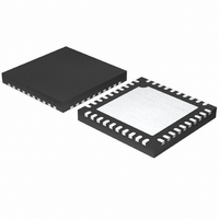
... Headphone/Line Audio Output (Output) - Stereo headphone or line level analog outputs Analog Power (Input) - Positive power for the internal analog section. 8 5/13/ GND/Thermal Pad 25 24 Top-Down (Through-Package) View 40-Pin QFN Package Pin Description CS42L52 AIN1B AIN1A AFILTB AFILTA AIN2B AIN2A AIN3B/MIC2-/MIC1B AIN3A/MIC1-/MIC1A AIN4B/MIC2+/MIC2B AIN4A/MIC1+/MIC2A DS680F1 ...
Page 9
... V - 3.47 V, CMOS (~1 MΩ) Weak Pullup 1. 3.47 V, CMOS (~1 MΩ 1 5.25 V Power MOSFET - 1 5.25 V Power MOSFET - 1 5.25 V Power MOSFET - 1 5.25 V Power MOSFET CS42L52 Receiver 1. 3.47 V, with Hysteresis 1. 3.47 V, with Hysteresis 1. 3.47 V, with Hysteresis 1. 3. 3. 3. 3. ...
Page 10
... AIN4A/MIC2A MICBIAS MIC2+ AIN4B/MIC2B MIC2- AIN3B/MIC1B AGND AFILTA AFILTB VQ FILT+ DGND Figure 1. Typical Connection Diagram CS42L52 +1 +2 µF See Note 5 Line Level Out 47 kΩ Left & Right 0.022 µF 51.1 Ω Headphone Out Left & Right 51.1 Ω 0.022 µF +1 ...
Page 11
... VA, VHP -0.3 Speaker VP -0.3 Digital VD -0.3 VL -0.3 (Note (Note 2) AGND-0 -VHP - 0 (Note 2) V -0.3 IND (power applied -65 stg CS42L52 Min Max Units 1.65 2.63 V 1.65 2.63 V 1.60 5.25 V 1.65 2.63 V 1.65 3.47 V °C -40 +85 °C -40 +105 Max Units 3 ...
Page 12
... Ω ADC 0.73•VA 0.769•VA 0.83•VA PGA (0 dB) 0.73•VA 0.770•VA 0.83•VA PGA (+12 dB) 0.194•VA MIC (+16 dB) 0.115•VA MIC (+32 dB) 0.019•VA ADC - 20 PGA - 39 MIC - 50 CS42L52 VA = 1.8V Max Min Typ Max - -80 - -84 - -73 - -30 - -33 - ...
Page 13
... Ω ADC 0.73•VA 0.769•VA 0.83•VA PGA (0 dB) 0.73•VA 0.770•VA 0.83•VA - 0.194•VA - 0.115•VA - 0.019•VA ADC 18 - PGA 40 - MIC 50 - CS42L52 Test Conditions (unless = - “Required Initial 1.65 - 1.89 V Min Typ Max - -78 - -84 - -73 - -28 - -33 - ...
Page 14
... Response is clock-dependent and will scale with Fs. Note that the response plots page 78) have been normalized to Fs and can be de-normalized by multiplying the X-axis scale by Fs. HPF parameters are for kHz. 14 5/13/08 (Note 5) to -0.1 dB corner -3.0 dB -0.13 dB CS42L52 Min Typ Max Unit 0 - 0.4948 Fs -0. ...
Page 15
... Refer to Table “Line Output Voltage Level Characteris- tics” on page 20 Refer to Table “Headphone Output Power Characteristics” on page 19 16 Ω kΩ 0.1 - ±100 (Note (Note CS42L52 = +25° kΩ for the line output L L “Required Initial 1.8 V Max Min Typ Max Unit - ...
Page 16
... Refer to the table in teristics” on page 20 (Note 7) Refer to the table in page 19 16 Ω kΩ 0.1 - ±100 (Note (Note reflect the recommended minimum resistance and maximum capacitance re- L CS42L52 = - kΩ for the headphone output 1.65 - 1.89 V Max Min Typ Max - ...
Page 17
... R L (Note 9) Symbol Conditions P O THD+N < 10% THD+N < 1% THD+N < 10% THD+N < 1% THD dBFS = 0. dBFS = 0. dBFS = 1 -60 dBFS, A-Weighted -60 dBFS, Unweighted -60 dBFS, A-Weighted -60 dBFS, Unweighted O CS42L52 VA = 1.8 V Min Typ Max - - - - - - - 0.91• 0.84• 0/-0 ...
Page 18
... THD+N < 1% THD dBFS = 0. dBFS = 0. dBFS = 0. -60 dBFS, A-Weighted -60 dBFS, Unweighted -60 dBFS, A-Weighted -60 dBFS, Unweighted 5.0V 0.5 A DS(ON 3.7V 0.5 A DS(ON 2.5V 0.5 A DS(ON) d η 5 0 RESET, pin 32, is held low VP CS42L52 Min Typ Max Units - 0. rms - 0. rms - 1. rms - 0. rms - ...
Page 19
... DS680F1 5/13/ Ω (see 2.5V Min Typ Max - (Note 11 (Note 11 (Note 7, 11) See Figures 22 AOUTx 51 Ω C 0.022 µF L AGND Figure 2. Headphone Output Test Load CS42L52 Figure 2); “Required Initialization Settings” 1.8V Min Typ Max - (Note 7), Figure 22 on page and 23 on page 74 ...
Page 20
... kHz Fs = 44.1 kHz kHz CS42L52 2); “Required Initialization Settings” 1.8V Unit Min Typ Max - 1.25 - 1.41 1.48 1. 1.73 - 2. ...
Page 21
... SDOUT Hold Time After SCLK Rising Edge SDIN Setup Time Before SCLK Rising Edge SDIN Hold Time After SCLK Rising Edge 14. After powering up the CS42L52, RESET should be held low after the power supplies and clocks are settled. 15. See “Example System Clock Frequencies” on page 76 ...
Page 22
... Repeated t high t t sud t sust low hdd Figure 4. Control Port Timing - I²C CS42L52 Min Max - 100 550 - 4.7 - 4.0 - 4.7 - 4 250 - - 1 - 300 4.7 - 300 1000 , of SCL. fc Stop Start t ...
Page 23
... BIASLVL[2:0] = 101 1 kHz PGA to ADC ADC DAC (HP & Line Amps) PGA to ADC (Note 18) ADC DAC (HP & Line Amps) Full-Bridge PWM Outputs (Note 19) Symbol > 2.0 V for serial and control port power rails. CS42L52 Min Typ Max - 0.5• 0.5• 0.6• ...
Page 24
... Initialization Settings” on page 37 CS42L52 Typical Current (mA VHP VL=3.3V VP=3.7V (Note 23) (mW 0 ...
Page 25
... The power MOSFETS are powered directly from a battery eliminating the efficiency loss associated with an external regulator. Battery level monitoring and compensation maintains a steady output as battery levels fall. NOTE: The CS42L52 should only be used in captive speaker systems where the outputs are permanently tied to the speaker terminals. ...
Page 26
... ADCBM UTE DIGSFT DIGZC PDN_ADCB HPFRZB ADCBVOL[7:0] INV_ADCB HPB +24/-96dB PDN_CHRG HPFB_CF[1:0] 1dB steps TO DSP Engine FROM DSP ENGINE Figure 5. Analog Input Signal Flow CS42L52 = PGAASEL[5:1] AIN1A AIN2A AIN3A/MIC1-/ Σ MIC1A AIN4A/ MIC1+/ MIC2A PDN_PGAA Refer to PGAAVOL[5:0] “M IC Inputs” ADCB=A ANLGSFTA ...
Page 27
... MIC2 summing MIC2+ 16..32 dB steps PGA B PDN_MICA=’0'b PDN_MICB=’0'b Note: Output to PGA = (MIC Figure 7. Differential MIC Configuration Register Location “MICx Configuration” on page 55 “Power Down MICx” on page 43 “MICx Gain” on page 55 CS42L52 MICAGAIN[4: summing 16..32 dB steps PGA A MICBGAIN[4: ...
Page 28
... Referenced Control Noise Gate Controls............ 28 5/13/ Figure 8. ALC Register Location “Noise Gate Control (Address 2Dh)” on page 69 Output (dB) -52 dB -64 dB -80 dB -96 -40 THRESH[2:0] Figure 9. Noise Gate Attenuation CS42L52 sca Input (dB) DS680F1 ...
Page 29
... VOL Channel ADCASWAP[1:0] Swap ADCBSWAP[1:0] PCMASWAP[1:0] PCMBSWAP[1:0] Σ Σ Channel Swap BPVOL[4:0] 0dB/-50dB 2.0dB steps Beep VOL Figure 10. DSP Engine Signal Flow CS42L52 LIMARATE[7:0] LIMRRATE[7:0] LMAX[2:0] CUSH[2:0] LIMSRDIS LIMZCDIS LIMIT Limiter Peak Detect Bass/ VOL Treble/ Control TC_EN MSTAMUTE BASS_CF[1:0] ...
Page 30
... HPA_VOL[7:0] HPB_VOL[7:0] +0dB/-102dB 0.5dB steps from DSP VOL Engine + Analog Passthru - from PGA Speaker Outputs Short Circuit Figure 12. Analog Output Stage CS42L52 PDN_HPA[1:0] PDN_HPB[1:0] HPGAIN[2:0] A DAC HP/Line Outputs B VOL Charge Pump PASSTHRUA PASSTHRUB PASSAMUTE PASSBMUTE CHGFREQ[3:0] PASSAVOL[7:0] PASSBVOL[70] +12dB/-60dB ...
Page 31
... Configuration” on page 61 “Beep Mix Disable” on page 61 “Beep Volume” on page 61 Register Location “Limiter Control 2, Release Rate (Address 28h)” on page “Master Volume Control: MSTA (Address 20h) & MSTB (Address 21h)” on page 63 CS42L52 ... 66, “Limiter Attack Rate (Address 29h)” on page 67 31 ...
Page 32
... To accommodate automatic activation of the speaker amplifier when the SPK/HP_SW switch pin chang- es, the CS42L52 provides the option to automatically power up the ADC whenever the analog signal must route to the digital PWM modulator, regardless of the PDN_ADC bit. Refer to the table below for details on how this ADC power-down override functions in accordance with the state of the speaker channels ...
Page 33
... SPKMONO.......................... SPKSWAP........................... 4.5.2 VP Battery Compensation The CS42L52 provides the option to maintain a desired power output level, independent of the VP supply. When enabled, this feature works by monitoring the voltage on the VP supply and reducing the attenua- tion on the speaker outputs when VP voltage levels fall. Note: The internal ADC that monitors the VP supply operates from the VA supply ...
Page 34
... Set speaker attenuation (SPKxVOL) to -10 dB. The VP supply changes ~9.9 dB. 2. Set the reference VP supply (VPREF Enable battery compensation (BATTCMP). The CS42L52 automatically adjusts the output level as the battery discharges. Refer to 34. In this example, the VP supply changes over a wide range, illustrating the accuracy of the CS42L52’s battery compensation ...
Page 35
... DS680F1 5/13/08 SPEED[1:0] 32kGROUP VIDEOCLK (AUTO=’0’ Table 1. MCLK, LRCK Quick Decode CS42L52 RATIO[1:0] MCLKDIV2 ...
Page 36
... The right channel immediately follows the left channel. LRCK SCLK SDIN Audio Word Length (AWL) 36 5/13/ Figure 16. I²S Format Figure 17. Left-Justified Format UTL Audio W ord Length (AW L) 1/fs L eft HP/LINE OUTA Figure 19. DSP Mode Format) CS42L52 AOUTB / AINxB MSB AOUTB / AINxB UTR HP/LINE OUTB DS680F1 MSB ...
Page 37
... Write 0x99 to register 0x00. 2. Write 0xBA to register 0x3E. 3. Write 0x80 to register 0x47. 4. Write ‘1’b to bit 7 in register 0x32. 5. Write ‘0’b to bit 7 in register 0x32. 6. Write 0x00 to register 0x00. DS680F1 5/13/08 42. Section 4.11. Section 4.6. CS42L52 37 ...
Page 38
... SDA while the clock is high. A Stop condition is defined as a rising transition of SDA while the clock is high. All other transitions of SDA occur while the clock is low. The first byte sent to the CS42L52 after a Start condition consists of a 7-bit chip address field and a R/W bit (high for a read, low for a write). ...
Page 39
... The device has MAP auto-increment capability enabled by the INCR bit (the MSB) of the MAP. If INCR is set to 0, MAP will stay constant for successive I²C writes or reads. If INCR is set to 1, MAP will auto-in- crement after each byte is read or written, allowing block reads or writes of successive registers. DS680F1 5/13/08 CS42L52 39 ...
Page 40
... PGAAVOL5 PGAAVOL4 PGAAVOL3 PGABVOL5 PGABVOL4 PGABVOL3 ADCAVOL5 ADCAVOL4 ADCAVOL3 ADCBVOL5 ADCBVOL4 ADCBVOL3 AMIXAVOL4 AMIXAVOL3 AMIXAVOL2 AMIXAVOL1 AMIXAVOL0 PMIXAVOL4 PMIXAVOL3 PMIXAVOL2 PMIXAVOL1 PMIXAVOL0 CS42L52 REVID2 REVID1 REVID0 PDN PDN_MICB PDN_MICA PDN_BIAS RATIO1 RATIO0 MCLKDIV2 DACDIF0 AWL1 AWL0 BIASLVL2 BIASLVL1 BIASLVL0 PGAASEL3 PGAASEL2 ...
Page 41
... ALCMIN2 NGBOOST THRESH2 THRESH1 DSPBOVFL DSPAOVFL PCMAOVFL PCMBOVFL ADCAOVFL Reserved Reserved VPLVL5 VPLVL4 SPKASHRT SPKBSHRT Reserved Reserved Reserved Reserved CHGFREQ1 CHGFREQ0 CS42L52 ONTIME3 ONTIME2 ONTIME1 BPVOL3 BPVOL2 BPVOL1 BASS_CF1 BASS_CF0 BASS3 BASS2 BASS1 MSTAVOL2 MSTAVOL1 MSTBVOL2 MSTBVOL1 HPAVOL3 HPAVOL2 HPAVOL1 HPBVOL3 ...
Page 42
... Powered Down Application “Analog In to Analog Out Passthrough” on page 32 Notes: 1. The CS42L52 employs a clever scheme for controlling the power to the PGA when PASSTHRU (“Passthrough Analog” on page 2. This bit should be used in conjunction with ADCxSEL and PGAxSEL bits to determine the analog 42 ...
Page 43
... Powered Down Application “Analog In to Analog Out Passthrough” on page 32 Notes: 1. The CS42L52 employs a clever scheme for controlling the power to the ADC when PASSTHRU (“Passthrough Analog” on page enabled. Refer to the referenced application. 6.2.4 Power Down Configures the power state of the entire CODEC. ...
Page 44
... Refer to the referenced application for more information. 44 5/13/ PDN_HPA0 PDN_SPKB1 32k_GROUP VIDEOCLK 45) and/or the VIDEOCLK bit (“Internal MCLK/LRCK Ratio” on page CS42L52 PDN_SPKB0 PDN_SPKA1 PDN_SPKA0 RATIO1 RATIO0 MCLKDIV2 (“27 MHz Video Clock” on 45). Low sample rates may also DS680F1 ...
Page 45
... MCLK/LRCK Ratio 512 256 128 128 “Master/Slave Mode” on page 45) and/or the VIDEOCLK bit (“Internal MCLK/LRCK Ratio” on page (“Auto-Detect” on page SCLK/LRCK Ratio in Master Mode CS42L52 SCLK/LRCK Ratio 46. (“27 MHz Video Clock” on 45). Low sample rates may also 44) is enabled. 45 ...
Page 46
... Select the audio word length using the AWL[1:0] bits 2. The interface format for both the ADC and the DAC must be set to “Left-Justified” when DSP Mode is enabled. 46 5/13/ DSP DACDIF1 (“Audio Word Length” on page CS42L52 (“Auto-Detect” on page 44) is disabled DACDIF0 AWL1 AWL0 47). DS680F1 0 ...
Page 47
... Configures an internal loops the signal on the SDOUT pin to SDIN. DIGLOOP Internal Loopback 0 Disabled; SDOUT internally disconnected from SDIN 1 Enabled; SDOUT internally connected to SDIN DS680F1 5/13/08 Right Justified (DAC ONLY) 24-bit data 20-bit data 18-bit data 16-bit data 3ST_SP INV_SWCH BIASLVL2 CS42L52 (“Audio Word Length” BIASLVL1 BIASLVL0 47 ...
Page 48
... Inputs” on page 26 48 5/13/08 “Master/Slave Mode” on page PGAASEL5 PGAASEL4 (“PGA Input Mapping” on page CS42L52 Master Mode Serial Port clocks and SDOUT are outputs Serial Port clocks and SDOUT are HI-Z 46 PGAASEL3 PGAASEL2 PGAASEL1 49) to select input channels ...
Page 49
... ANLGSFTB Affected Analog Volume Controls MICxGAIN[4:0] (“MICx Gain” on page on page 56), and PASSxVOL[7:0] Affected Analog Volume Controls MICxGAIN[4:0] (“MICx Gain” on page on page 56), and PASSxVOL[7:0] CS42L52 ) to select MIC 1 or MIC 2; for ) ANLGZCB ANLGSFTA ANLGZCA 55), PGAxVOL[5:0] (“PGAx Volume” (“Passthrough x Volume” on page ...
Page 50
... Affected Volume Controls ADCxVOL[7:0] (“ADCx Volume” on page ADCxMUTE (“ADC Mute” on page ALC and Limiter Attack/Release MICxGAIN[4:0] (“MICx Gain” on page PGAxVOL[5:0] (“PGAx Volume” on page PASSxVOL[7:0] (“Passthrough x Volume” on page CS42L52 2 1 HPFB_CF0 HPFA_CF1 HPFA_CF0 2 1 INV_ADCA ADCBMUTE ADCAMUTE 57), ...
Page 51
... Control 2 (Address 0Fh)” on page AMIXxVOL[7:0] (“ADC Mixer Channel x Volume” on page PMIXxVOL[7:0] (“PCM Mixer Channel x Volume” on page MSTxVOL[7:0] (“Master Volume Control” on page HPxVOL[7:0] (“Headphone Volume Control” on page CS42L52 INV_PCMA MSTBMUTE MSTAMUTE and “Headphone Output Power 54), ...
Page 52
... Modifications may be made to all control port registers without the changes taking effect until after the 1 FREEZE is disabled. 52 5/13/08 (“Digital Soft Ramp” on page 53) bits FREEZE 56) and the headphone amplifier volume control settings (hidden). When CS42L52 53) and DIGZC DEEMPH DIGSFT DIGZC DS680F1 ...
Page 53
... ALC and Limiter Attack/Release Beep Volume (“Beep Volume” on page (“Limiter Soft Ramp Disable” on page bits 7 and 6 in register 29h are set to ‘00’b. CS42L52 52), (“Playback Control 2 (Address 0Fh)” on page 57), (“ADC Mixer Channel x Volume” on page (“PCM Mixer Channel x Volume” on page ...
Page 54
... Disabled; The PWM amplifiers outputs modulated silence when SPKxMUTE is enabled. Enabled; The PWM amplifiers switch at an exact 50%-duty-cycle signal (not modulated) when SPKxMUTE is 1 enabled. 54 5/13/ SPKAMUTE SPKB=A Affected Volume Controls SPKxMUTE (“Speaker Mute” on page SPKxVOL[7:0] (“Speaker Volume Control” on page CS42L52 SPKSWAP SPKMONO MUTE50/50 54), 64) DS680F1 ...
Page 55
... OFF; ALC Attack Rate is dictated by the ANLGSFT 1 ON; ALC volume changes take effect in one step, regardless of the ANLGSFT setting. Application: “Automatic Level Control (ALC)” on page 27 DS680F1 5/13/ MICxGAIN4 MICxGAIN3 PGAxVOL4 PGAxVOL3 (“Ch. x Analog Soft Ramp” on page CS42L52 MICxGAIN2 MICxGAIN1 MICxGAIN0 PGAxVOL2 PGAxVOL1 PGAxVOL0 49) setting 55 ...
Page 56
... Step Size: 0.5 dB Note: The PGAxVOL bits are ignored when the PASSTHRUx bit enabled. 56 5/13/08 (“Ch. x Analog Zero Cross” on page (“Passthrough Analog” on page CS42L52 49) setting 52) is DS680F1 ...
Page 57
... Step Size: 1.0 dB DS680F1 5/13/ PASSxVOL4 PASSxVOL3 (“Passthrough Analog” on page ADCAVOL4 ADCAVOL3 CS42L52 PASSxVOL2 PASSxVOL1 PASSxVOL0 52) is disabled ADCAVOL2 ADCAVOL1 ADCAVOL0 57 ...
Page 58
... Sets the volume/gain of the PCM mix from the serial data input (SDIN) to the DSP. PMIXxVOL[6:0] Volume 001 1000 +12.0 dB ... ... 000 0001 +0.5 dB 000 0000 0 dB 111 1111 -0.5 dB ... ... 001 1001 -51.5 dB Step Size: 0 5/13/ AMIXxVOL4 AMIXxVOL3 PMIXxVOL4 PMIXxVOL3 CS42L52 AMIXxVOL2 AMIXxVOL1 AMIXxVOL0 PMIXxVOL2 PMIXxVOL1 PMIXxVOL0 DS680F1 ...
Page 59
... Hz Application: “Beep Generator” on page 30 Notes: 1. This setting must not change when BEEP is enabled. 2. Beep frequency will scale directly with sample rate, Fs, but is fixed at the nominal Fs within each speed mode. DS680F1 5/13/ FREQ0 ONTIME3 CS42L52 2 1 ONTIME2 ONTIME1 ONTIME0 Pitch ...
Page 60
... Application: “Beep Generator” on page 30 Notes: 1. This setting must not change when BEEP is enabled. 2. Beep off time will scale inversely with sample rate, Fs, but is fixed at the nominal Fs within each speed mode. 60 5/13/ BPVOL4 BPVOL3 CS42L52 BPVOL2 BPVOL1 BPVOL0 DS680F1 ...
Page 61
... Mix Disabled; The output alternates between the signal from the serial data input and the beep signal. The 1 beep signal does not mix with the digital signal from the serial data input. Application: “Beep Generator” on page 30 Note: This setting must not change when BEEP is enabled. DS680F1 5/13/ TREBCF1 TREBCF0 CS42L52 BASSCF1 BASSCF0 TCEN 61 ...
Page 62
... Sets the gain of the treble shelving filter. TREB[3:0] Gain Setting 0000 +12.0 dB ··· ··· 0111 +1.5 dB 1000 0 dB 1001 -1.5 dB ··· ··· 1111 -10.5 dB Step Size: 1 5/13/ TREB0 BASS3 CS42L52 BASS2 BASS1 BASS0 DS680F1 ...
Page 63
... Muted Step Size: 0.5 dB DS680F1 5/13/ MSTxVOL4 MSTxVOL3 HPxVOL4 HPxVOL3 CS42L52 MSTxVOL2 MSTxVOL1 MSTxVOL0 HPxVOL2 HPxVOL1 HPxVOL0 63 ...
Page 64
... Configures a mix/swap of the ADC Mix to the headphone/line or speaker outputs. ADCxSWP[1:0] ADC Mix to HP/LINEOUTA Channel 00 Left 01 (Left + Right)/ Right 64 5/13/ SPKxVOL4 SPKxVOL3 PCMBSWP0 ADCASWP1 CS42L52 2 1 SPKxVOL2 SPKxVOL1 SPKxVOL0 2 1 ADCASWP0 ADCBSWP1 ADCBSWP0 PCM Mix to HP/LINEOUTB Right (Left + Right)/2 Left ADC Mix to HP/LINEOUTB Channel Right (Left + Right)/2 Left DS680F1 0 0 ...
Page 65
... Note: This bit is ignored when the DIGZC DS680F1 5/13/ CUSH2 CUSH1 66). 66) until levels lie between the LMAX and CUSH thresholds. (“Digital Soft Ramp” on page (“Digital Zero Cross” on page CS42L52 CUSH0 LIMSRDIS LIMZCDIS 53) setting 53) is enabled. 65 ...
Page 66
... The limiter release rate is user-selectable but is also a function of the sampling frequency, Fs, and the DIGSFT (“Digital Soft Ramp” on page 66 5/13/08 (“Digital Zero Cross” on page LIMRRATE4 LIMRRATE3 65) and returns the analog output level to the MSTxVOL[7:0] 63) setting. 53) and DIGZC CS42L52 53) setting LIMRRATE2 LIMRRATE1 LIMRRATE0 (“Digital Zero Cross” on page 53) setting. DS680F1 ...
Page 67
... LIMARATE3 65). 53) and DIGZC (“Digital Zero Cross” on page (“Limiter Soft Ramp Disable” on page AALCRATE4 ALCARATE3 68). 49) and ANLGZCx (“ALCx Soft Ramp Disable” on page 55 56) is enabled. CS42L52 LIMARATE2 LIMARATE1 LIMARATE0 53) setting unless or “Limiter Zero Cross Disable” ALCARATE2 ALCARATE1 ALCARATE0 (“ ...
Page 68
... Level Control (ALC)” on page 27 68 5/13/ ALCRRATE4 ALCRRATE3 69) and returns the signal level to the PGAx- 56) and ADCxVOL[7:0] 49) and ANLGZCx ALCMIN2 ALCMIN1 67). CS42L52 2 1 ALCRRATE2 ALCRRATE1 ALCRRATE0 (“ADCx Volume” on page 57) setting. (“Ch. x Analog Zero Cross” ALCMIN0 Reserved Reserved 0 0 DS680F1 ...
Page 69
... Gate” on page 28 6.35.2 Noise Gate Enable Configures the noise gate. NG Noise Gate Status 0 Disabled 1 Enabled Application: “Noise Gate” on page 28 DS680F1 5/13/08 “ALC Release Rate” on page 68) until levels lie between the ALCMAX and AL THRESH2 THRESH1 CS42L52 THRESH0 NGDELAY1 NGDELAY0 69 ...
Page 70
... On initial power up and application of clocks, this bit will report ‘1’b as the serial port re-synchro- nizes. 70 5/13/08 49) and ANLGZCx (“Ch. x Analog Zero Cross” on page (“ALCx Soft Ramp Disable” on page DSPBOVFL PCMAOVFL CS42L52 Minimum Setting (NG_BOOST = ‘1’b) -34 dB -37 dB -40 dB -43 dB -46 dB -52 dB -58 dB -64 dB 49) setting unless or “ ...
Page 71
... VPMONITOR setting. Conversely, when BATTCMP is disabled, the ADC may be enabled by enabling VPMONITOR; this provides a convenient battery monitor without enabling battery compensation. 2. When enabled, VPMONITOR remains enabled regardless of the PDN bit setting. DS680F1 5/13/ Reserved VPREF3 CS42L52 (“PCM Mixer Channel x Volume” on page VPREF2 VPREF1 VPREF0 58) 71 ...
Page 72
... Speaker Current Load Status (Read Only) Indicates whether or not any of the speaker outputs is shorted to ground. SPKxSHRT Speaker Output Load 0 No overload detected 1 Overload detected 72 5/13/08 (for VA = 1.8 V) (for VPLVL4 VPLVL3 SPKBSHRT SPKR/HP CS42L52 VPLVL2 VPLVL1 VPLVL0 Reserved Reserved Reserved DS680F1 ...
Page 73
... Charge Pump Frequency (Address 34h CHGFREQ3 CHGFREQ2 CHGFREQ1 6.40.1 Charge Pump Frequency Sets the charge pump frequency on FLYN and FLYP. CHGFREQ[3:0] N 0000 0 ... 0101 5 ... 1111 15 Formula: Frequency = (64xFs)/(N+2) Note: The headphone output THD+N performance may be affected. DS680F1 5/13/ CHGFREQ0 Reserved CS42L52 Reserved Reserved Reserved 73 ...
Page 74
... W 40m 50m 60m 70m 80m W CS42L52 G = 0.6047 G = 0.7099 G = 0.8399 G = 1.0000 G = 1.1430 Legend NOTE: Graph shows the out- put power per channel (i.e. Output Power = 23 mW into single 16 Ω and 46 mW into stereo 16 Ω with THD dB) ...
Page 75
... W 30m 35m 40m 45m 50m 55m 60m W CS42L52 G = 0.6047 G = 0.7099 G = 0.8399 G = 1.0000 G = 1.1430 Legend NOTE: Graph shows the out- put power per channel (i.e. Output Power = 22 mW into single 32 Ω and 44 mW into stereo 32 Ω with THD dB) ...
Page 76
... MCLK (MHz) 256x 384x 8.1920 12.2880 11.2896 16.9344 12.2880 18.4320 MCLK (MHz) 128x 192x 8.1920 12.2880 11.2896 16.9344 12.2880 18.4320 CS42L52 2048x* 3072x* 16.3840 24.5760 22.5792 33.8688 24.5760 36.8640 1024x* 1536x* 16.3840 24.5760 22.5792 33.8688 24.5760 36.8640 512x* 768x* 16.3840 24 ...
Page 77
... QFN Thermal Pad The CS42L52 is available in a compact QFN package. The underside of the QFN package reveals a large metal pad that serves as a thermal relief to provide for maximum heat dissipation. This pad must mate with an equally dimensioned copper pad on the PCB and must be electrically connected to ground. A series of vias should be used to connect this copper pad to one or more larger ground planes on other PCB layers ...
Page 78
... DAC DIGITAL FILTERS Figure 26. ADC Passband Ripple Figure 28. ADC Transition Band Figure 30. DAC Passband Ripple Figure 32. DAC Transition Band 78 5/13/08 Figure 27. ADC Stopband Rejection Figure 29. ADC Transition Band (Detail) Figure 31. DAC Stopband Figure 33. DAC Transition Band (Detail) CS42L52 DS680F1 ...
Page 79
... The gain difference between left and right channel pairs. Units in decibels. Gain Drift The change in gain value with temperature. Units in ppm/°C. Offset Error The deviation of the mid-scale transition (111...111 to 000...000) from the ideal. Units in mV. DS680F1 5/13/08 CS42L52 79 ...
Page 80
... MIN -- 0.0394 -- -- 0.0020 0.00 0.0110 0.18 0.1634 4.05 0.1634 4.05 0.0197 0.30 JEDEC #: MO-220 Controlling Dimension is Millimeters. Symbol 2 Layer Board 4 Layer Board CS42L52 b e PIN #1 CORNER D2 MILLIMETERS NOM MAX -- 1.00 -- 0.05 0.23 0.28 6.00 BSC 4.10 4.15 6.00 BSC 4.10 4.15 ...
Page 81
... Volume Setting B=A” on page “MICx Gain” on page 55. 71. CS42L52 Container Order # Rail CS42L52-CNZ Tape & Reel CS42L52-CNZR Rail CS42L52-DNZ Tape & Reel CS42L52-DNZR - - CDB42L52 - - CRD42L52 9. 24. “Automatic Level Control (ALC)” on “Required Initialization Settings” on page “ ...
Page 82
... TORNEYS’ FEES AND COSTS, THAT MAY RESULT FROM OR ARISE IN CONNECTION WITH THESE USES. Cirrus Logic, Cirrus, and the Cirrus Logic logo designs are trademarks of Cirrus Logic, Inc. All other brand and product names in this document may be trademarks or service marks of their respective owners. I² registered trademark of Philips Semiconductor. 82 5/13/08 CS42L52 DS680F1 ...