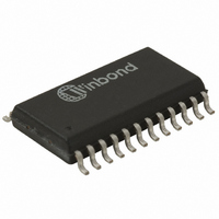
W6811ISG TR Nuvoton Technology Corporation of America, W6811ISG TR Datasheet - Page 10

W6811ISG TR
Manufacturer Part Number
W6811ISG TR
Description
IC VOICEBAND CODEC 5V/3V 24SOP
Manufacturer
Nuvoton Technology Corporation of America
Type
PCMr
Datasheet
1.W6811IE.pdf
(37 pages)
Specifications of W6811ISG TR
Data Interface
PCM Audio Interface
Resolution (bits)
8 b
Number Of Adcs / Dacs
1 / 1
Sigma Delta
No
Voltage - Supply, Analog
4.5 V ~ 5.5 V
Voltage - Supply, Digital
2.7 V ~ 3.3 V
Operating Temperature
-40°C ~ 85°C
Mounting Type
Surface Mount
Package / Case
24-SOP
For Use With
W6811DK - KIT DEVELOPMENT FOR W6811
Lead Free Status / RoHS Status
Lead free / RoHS Compliant
Other names
W6811ISG T&R
W6811ISG T&R
W6811ISG T&R
The power supply for the analog part of the W6811 needs to be 5V +/- 10%. This supply voltage is
connected to the V
capacitor.
The power supply for the digital part of the W6811 needs to be 3V +/- 10%. This supply voltage is
connected to the V
capacitor.
The system has an internal precision voltage reference which generates the 2.5V mid-supply analog
ground voltage. This voltage needs to be decoupled to V
capacitor.
The analog ground reference voltage is available for external reference at the V
needs to be decoupled to V
voltage is generated from the voltage on the V
processing.
The PCM interface is controlled by pins BCLKR, FSR, BCLKT & FST. The input data is received
through the PCMR pin and the output data is transmitted through the PCMT pin. The modes of
operation of the interface are shown in Table 7.3.
Table 7.3 PCM Interface mode selections
The Long Frame Sync or Short Frame Sync interface mode can be selected by connecting the BCLKR
or BCLKT pin to a 64 kHz to 4.096 MHz clock and connecting the FSR or FST pin to the 8 kHz frame
sync. The device synchronizes the data word for the PCM interface and the CODEC sample rate on
the positive edge of the Frame Sync signal. It recognizes a Long Frame Sync when the FST pin is
7.3. P
7.4. PCM I
7.3.1. Analog Supply
7.3.2. Digital Supply
7.3.3. Analog Ground Reference Bypass
7.3.4. Analog Ground Reference Voltage Output
7.4.1. Long Frame Sync
OWER
NTERFACE
BCLKR
64 kHz to 4.096
MHz
V
V
V
V
SSD
SSD
DDD
DDD
M
DDA
DDD
ANAGEMENT
pin. The V
pin. The V
SSA
through a 0.01 μF ceramic capacitor. The analog ground reference
DDA
DDD
pin needs to be decoupled to ground through a 0.1 μF ceramic
pin needs to be decoupled to ground through a 0.1 μF ceramic
FSR
8 kHz
V
V
V
V
SSD
DDD
SSD
DDD
REF
pin and is also used for the internal signal
Interface Mode
Long or Short Frame Sync
ISDN GCI with active channel B1
ISDN GCI with active channel B2
ISDN IDL with active channel B1
ISDN IDL with active channel B2
- 10 -
SSA
at the V
Publication Release Date: September, 2005
REF
pin through a 0.1 μF ceramic
AG
pin. This voltage
W6811
Revision A12


