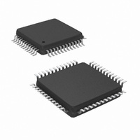
LM4549BVH/NOPB National Semiconductor, LM4549BVH/NOPB Datasheet - Page 17

LM4549BVH/NOPB
Manufacturer Part Number
LM4549BVH/NOPB
Description
IC AUDIO CODEC 2MULTICH 48-LQFP
Manufacturer
National Semiconductor
Datasheet
1.LM4549BVHNOPB.pdf
(28 pages)
Specifications of LM4549BVH/NOPB
Lead Free Status / RoHS Status
Lead free / RoHS Compliant
Other names
LM4549BVH
Available stocks
Company
Part Number
Manufacturer
Quantity
Price
Company:
Part Number:
LM4549BVH/NOPB
Manufacturer:
Texas Instruments
Quantity:
10 000
Functional Description
REGISTER RESET is performed when any value is written
to the RESET register, 00h. It resets all registers to their
AC Link Serial Interface Protocol
AC LINK OUTPUT FRAME:
SDATA_OUT, CONTROLLER OUTPUT TO LM4549B INPUT
The AC Link Output Frame carries control and PCM data to
the LM4549B control registers and stereo DAC. Output
Frames are carried on the SDATA_OUT signal which is an
output from the AC ’97 Digital Controller and an input to the
LM4549B codec. As shown in Figure 3, Output Frames are
constructed from thirteen time slots: one Tag Slot followed by
twelve Data Slots. Each Frame consists of 256 bits with each
of the twelve Data Slots containing 20 bits. Input and Output
Frames are aligned to the same SYNC transition. Note that
since the LM4549B is a two channel codec, it only accepts
data in 4 of the twelve Data Slots – 2 for control, one each for
PCM data to the left and right channel DACs. Data Slot 3 &
4 are used to stream data to the stereo DAC for all modes
selected by the Identity pins ID1#, ID0#.
A new Output Frame is signaled with a low-to-high transition
of SYNC. SYNC should be clocked from the controller on a
FIGURE 3. AC Link Bidirectional Audio Frame
(Continued)
FIGURE 4. AC Link Output Frame
17
default state and will modify circuit configurations accord-
ingly but does not reset any other internal circuits.
rising edge of BIT_CLK and, as shown in Figure 4 and
Figure 5, the first tag bit in the Frame (“Valid Frame”) should
be clocked from the controller by the next rising edge of
BIT_CLK and sampled by the LM4549B on the following
falling edge. The AC ’97 Controller should always clock data
to SDATA_OUT on a rising edge of BIT_CLK and the
LM4549B always samples SDATA_OUT on the next falling
edge. SYNC is sampled with the falling edge of BIT_CLK.
The LM4549B checks each Frame to ensure 256 bits are
received. If a new Frame is detected (a low-to-high transition
on SYNC) before 256 bits are received from the old Frame
then the new Frame is ignored i.e. the data on SDATA_OUT
is discarded until a valid new Frame is detected.
The LM4549B expects to receive data MSB first, in an MSB
justified format.
20123506
20123504
www.national.com


