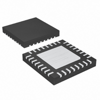
MAX9867ETJ+ Maxim Integrated Products, MAX9867ETJ+ Datasheet - Page 47

MAX9867ETJ+
Manufacturer Part Number
MAX9867ETJ+
Description
IC STEREO AUD CODEC LP 32TQFN-EP
Manufacturer
Maxim Integrated Products
Type
Stereo Audior
Datasheet
1.MAX9867EWVT.pdf
(55 pages)
Specifications of MAX9867ETJ+
Data Interface
I²C, Serial
Resolution (bits)
18 b
Number Of Adcs / Dacs
2 / 2
Sigma Delta
Yes
Dynamic Range, Adcs / Dacs (db) Typ
85 / 90
Voltage - Supply, Analog
1.65 V ~ 1.95 V
Voltage - Supply, Digital
1.65 V ~ 1.95 V
Operating Temperature
-40°C ~ 85°C
Mounting Type
Surface Mount
Package / Case
32-WFQFN Exposed Pad
Lead Free Status / RoHS Status
Lead free / RoHS Compliant
The MAX9867 recognizes a STOP condition at any
point during data transmission except if the STOP con-
dition occurs in the same high pulse as a START condi-
tion. For proper operation, do not send a STOP
condition during the same SCL high pulse as the
START condition.
The slave address is defined as the 7 most significant
bits (MSBs) followed by the read/write bit. For the
MAX9867, the 7 most significant bits are 0011000.
Setting the read/write bit to 1 (slave address = 0x31)
configures the MAX9867 for read mode. Setting the
read/write bit to 0 (slave address = 0x30) configures
the MAX9867 for write mode. The address is the first
byte of information sent to the MAX9867 after the
START condition.
The acknowledge bit (ACK) is a clocked 9th bit that the
MAX9867 uses to handshake receipt each byte of data
when in write mode (see Figure 11). The MAX9867 pulls
Figure 11. Acknowledge
Figure 12. Writing 1 Byte of Data to the MAX9867
S
SLAVE ADDRESS
ACKNOWLEDGE FROM MAX9867
______________________________________________________________________________________
SDA
SCL
CONDITION
Ultra-Low Power Stereo Audio Codec
START
R/W
Early STOP Conditions
0
A
Slave Address
Acknowledge
1
ACKNOWLEDGE FROM MAX9867
2
REGISTER ADDRESS
NOT ACKNOWLEDGE
down SDA during the entire master-generated 9th clock
pulse if the previous byte is successfully received.
Monitoring ACK allows for detection of unsuccessful
data transfers. An unsuccessful data transfer occurs if
a receiving device is busy or if a system fault has
occurred. In the event of an unsuccessful data transfer,
the bus master retries communication. The master pulls
down SDA during the 9th clock cycle to acknowledge
receipt of data when the MAX9867 is in read mode. An
acknowledge is sent by the master after each read byte
to allow data transfer to continue. A not acknowledge is
sent when the master reads the final byte of data from
the MAX9867, followed by a STOP condition.
A write to the MAX9867 includes transmission of a
START condition, the slave address with the R/W bit set
to 0, 1 byte of data to configure the internal register
address pointer, 1 or more bytes of data, and a STOP
condition. Figure 12 illustrates the proper frame format
for writing 1 byte of data to the MAX9867. Figure 13
illustrates the frame format for writing n bytes of data to
the MAX9867.
ACKNOWLEDGE
ACKNOWLEDGMENT
CLOCK PULSE FOR
9
A
B7
B6
ACKNOWLEDGE FROM MAX9867
B5
DATA BYTE
B4
1 BYTE
B3
B2
REGISTER ADDRESS POINTER
Write Data Format
AUTOINCREMENT INTERNAL
B1
B0
A
P
47


