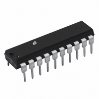
TP3069N National Semiconductor, TP3069N Datasheet - Page 5

TP3069N
Manufacturer Part Number
TP3069N
Description
IC INTERFACE ENHANCED SER 20-DIP
Manufacturer
National Semiconductor
Series
COMBO®r
Type
PCM Codec/Filterr
Datasheet
1.TP3069N.pdf
(18 pages)
Specifications of TP3069N
Data Interface
PCM Audio Interface
Resolution (bits)
8 b
Number Of Adcs / Dacs
1 / 1
Sigma Delta
No
Voltage - Supply, Analog
4.75 V ~ 5.25 V
Voltage - Supply, Digital
4.75 V ~ 5.25 V
Operating Temperature
-25°C ~ 125°C
Mounting Type
Through Hole
Package / Case
20-DIP (0.300", 7.62mm)
Lead Free Status / RoHS Status
Contains lead / RoHS non-compliant
Other names
*TP3069N
Symbol
POWER DISSIPATION (ALL DEVICES)
I
I
I
I
DIGITAL INTERFACE
V
V
V
V
I
I
I
CC
BB
CC
BB
IL
IH
OZ
Absolute Maximum Ratings
If Military Aerospace specified devices are required
please contact the National Semiconductor Sales
Office Distributors for availability and specifications
V
V
Voltage at any Analog Input
Electrical Characteristics
a
are assured by correlation with other production tests and or product design and characterization All signals referenced to
GNDA Typicals specified at V
Note
IL
IH
OL
OH
CC
BB
0
0
1
1
or Output
5 0V
to GNDA
to GNDA
I
CC0
g
5% V
Power-Down Current
Power-Down Current
Active Current
Active Current
Input Low Voltage
Input High Voltage
Output Low Voltage
Output High Voltage
Input Low Current
Input High Current
Output Current in High Impedance
State (TRI-STATE)
and I
BB0
BB
are measured after first achieving a power-up state
e b
Parameter
5 0V
g
CC
5% T
e a
V
CC
A
a
5 0V V
e
0 3V to V
0 C to 70 C by correlation with 100% electrical testing at T
Unless otherwise noted limits printed in BOLD characters are guaranteed for V
BB
(Note )
(Note )
VPI
VPI
D
TS
D
GNDA
V
D
IH s
X
X
X
BB
e b
X
e
e
I
I
GNDA
L
H
b
I
V
0V VF
0V VF
e
L
eb
s
b
IN s
0 3V
e
5 0V T
3 2 mA
V
7V
7V
3 2 mA Open Drain
IN s
3 2 mA
s
V
CC
R
R
V
O VPO
O VPO
O s
V
A
5
IL
Conditions
e
V
All Digital Inputs
CC
Voltage at any Digital Input
Operating Temperature Range
Storage Temperature Range
Lead Temp (Soldering 10 sec )
ESD (Human Body Model) J
ESD (Human Body Model) N
Latch-Up Immunity on Any Pin
25 C
or Output
a
a
and VPO
and VPO
b
b
unloaded
unloaded
b
b
b
Min
2 2
2 4
10
10
10
V
CC
A
a
e
0 05
Typ
0 3V to GNDA
0 5
7 0
7 0
25 C All other limits
b
b
25 C to
65 C to
10 0
10 0
Max
1 5
0 3
0 6
0 4
0 4
10
10
10
a
a
100 mA
b
1000V
1500V
125 C
150 C
300 C
CC
0 3V
Units
mA
mA
mA
mA
V
V
V
V
V
e
A
A
A


