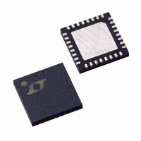
LTC1955EUH Linear Technology, LTC1955EUH Datasheet - Page 6

LTC1955EUH
Manufacturer Part Number
LTC1955EUH
Description
IC INTERFACE DL SMART CARD 32QFN
Manufacturer
Linear Technology
Datasheet
1.LTC1955EUHPBF.pdf
(20 pages)
Specifications of LTC1955EUH
Controller Type
Smart Card Interface
Interface
4-Wire Serial
Voltage - Supply
1.7 V ~ 5.5 V
Current - Supply
10µA
Operating Temperature
-40°C ~ 85°C
Mounting Type
Surface Mount
Package / Case
32-QFN
Lead Free Status / RoHS Status
Contains lead / RoHS non-compliant
Available stocks
Company
Part Number
Manufacturer
Quantity
Price
Company:
Part Number:
LTC1955EUH
Manufacturer:
LT
Quantity:
10 000
Part Number:
LTC1955EUH
Manufacturer:
LINEAR/凌特
Quantity:
20 000
Company:
Part Number:
LTC1955EUH#PBF
Manufacturer:
ADI
Quantity:
5
Part Number:
LTC1955EUH#PBF
Manufacturer:
LINEAR/凌特
Quantity:
20 000
Part Number:
LTC1955EUH#TRPBF
Manufacturer:
LINEAR/凌特
Quantity:
20 000
LTC1955
TYPICAL PERFORMANCE CHARACTERISTICS
PIN FUNCTIONS
SV
LTC1955.
PV
DV
SGND: Ground. Signal ground for analog sections of the
LTC1955. The Exposed Pad must be soldered to PCB
ground.
PGND: Ground. Power ground for the charge pump. This
pin should be connected directly to a low impedance
ground plane.
CPO: Charge Pump. CPO is the output of the charge pump.
When one or both of the smart cards requires power, the
charge pump will charge CPO to either 3.7V or 5.35V
depending on what smart card voltages are required. A
low impedance 4.7μF X5R or X7R ceramic capacitor is
required on CPO.
C
A 1μF X5R or X7R ceramic capacitor should be connected
from C
DATA: Input/Output. Microcontroller side data I/O pin. The
DATA pin provides the bidirectional communication path
to both smart cards. One, both or neither of the cards may
be selected to communicate via the DATA pin. If several
LTC1955s are connected in parallel, the DATA pin can be
made high impedance by selecting neither card. The C4A
6
5V/DIV
5V/DIV
5V/DIV
+
, C
V
BATT
BATT
V
I/O A
CC
CPO
CCA
: Power. Reference voltage for the control logic.
–
Charge Pump and LDO Activation
: Charge Pump. Charge pump fl ying capacitor pins.
: Power. Supply voltage for analog sections of the
: Power. Supply voltage for the charge pump.
+
to C
–
.
1ms/DIV
1955 G10
5V/DIV
5V/DIV
5V/DIV
5V/DIV
RST A
CLK A
I/O A
V
CCA
Deactivation Sequence
10μs/DIV
and C8A synchronous card pins can be selected to connect
to the DATA pin via the serial port (see Table 4).
R
smart cards. It is level shifted and transmitted directly
to the RST pin of a selected card socket. When a card is
deselected, the RST A/RST B pin for that channel is latched
at its current state.
SYNC: Input. The SYNC pin provides the clock input for
synchronous smart cards. When a synchronous card
is selected, its CLK pin follows SYNC directly. When a
synchronous card is deselected, the CLK A/CLK B pin for
that channel is latched at its current state.
ASYNC: Input. The ASYNC pin provides the clock input
for asynchronous cards and should be connected to a free
running clock. The clock signal to the smart card can be
a ÷1, ÷2, ÷4 or ÷8 version of the signal on ASYNC. Asyn-
chronous cards can also be placed in clock stop mode
with the clock stopped either high or low.
D
shifted into D
connected directly to a microcontroller or the D
another LTC1955 for daisychained operation.
D
data is shifted out of D
can be connected directly to a microcontroller or the D
pin of another LTC1955 for daisychained operation.
IN
IN
OUT
: Input. The R
: Input. Input for the serial port. Command data is
: Output. Output for the serial port. Smart card status
1955 G11
IN
synchronously with SCLK. D
IN
pin supplies the RST signal to both
2V/DIV
2V/DIV
OUT
DATA
I/O A
synchronously with SCLK. D
Data – I/O Channel, C
100ns/DIV
L
= 50pF
IN
OUT
can be
pin of
1955 G12
1955fb
OUT
IN


