SJA1000T/N1,118 NXP Semiconductors, SJA1000T/N1,118 Datasheet - Page 51
SJA1000T/N1,118
Manufacturer Part Number
SJA1000T/N1,118
Description
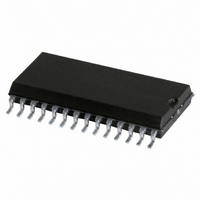
IC STAND-ALONE CAN CTRLR 28-SOIC
Manufacturer
NXP Semiconductors
Datasheet
1.SJA1000TN1112.pdf
(68 pages)
Specifications of SJA1000T/N1,118
Package / Case
28-SOIC (7.5mm Width)
Controller Type
CAN Interface
Interface
CAN
Voltage - Supply
4.5 V ~ 5.5 V
Current - Supply
15mA
Operating Temperature
-40°C ~ 125°C
Mounting Type
Surface Mount
Product
Controller Area Network (CAN)
Number Of Transceivers
1
Data Rate
1 Mbps
Frequency
24 MHz
Supply Voltage (max)
5.5 V
Supply Voltage (min)
4.5 V
Supply Current (max)
15 mA
Maximum Operating Temperature
+ 125 C
Minimum Operating Temperature
- 40 C
Mounting Style
SMD/SMT
Package
28SO
Maximum Data Rate
1 Mbps
Minimum Single Supply Voltage
4.5 V
Standard Supported
CAN 2.0B
Power Down Mode
Sleep
Maximum Single Supply Voltage
5.5 V
Lead Free Status / RoHS Status
Lead free / RoHS Compliant
Lead Free Status / RoHS Status
Lead free / RoHS Compliant, Lead free / RoHS Compliant
Other names
568-1123-2
935230920118
SJA1000TD-T
935230920118
SJA1000TD-T
Available stocks
Company
Part Number
Manufacturer
Quantity
Price
Company:

Part Number:
SJA1000T/N1,118
Manufacturer:
XILINX
Quantity:
125
Part Number:
SJA1000T/N1,118
Manufacturer:
NXP/恩智浦
Quantity:
20 000


Philips Semiconductors
6.5.2.2
TSEG1 and TSEG2 determine the number of clock cycles per bit period and the location of the sample point, where:
t
t
t
6.5.3
The output control register allows the set-up of different
output driver configurations under software control.
Table 46 Bit interpretation of the output control register (OCR); CAN address 8
2000 Jan 04
SYNCSEG
TSEG1
TSEG2
handbook, full pagewidth
Stand-alone CAN controller
Possible values are BRP = 000001, TSEG1 = 0101 and TSEG2 = 010.
OCTP1
BIT 7
= t
= t
O
scl
scl
= 1
XTAL
UTPUT
Time Segment 1 (TSEG1) and Time Segment 2 (TSEG2)
CAN
(8
(4
t
scl
C
TSEG1.3 + 4
TSEG2.2 + 2
OCTN1
ONTROL
BIT 6
SYNC
SEG
t SYNCSEG
t scl
R
EGISTER
OCPOL1
t CLK
TSEG1.2 + 2
TSEG2.1 + TSEG2.0 + 1)
BIT 5
t TSEG1
TSEG1
nominal bit time
(OCR)
Fig.13 General structure of a bit period.
sample point(s)
Baud Rate Prescaler (BRP)
OCTP0
BIT 4
TSEG1.1 + TSEG1.0 + 1)
t TSEG2
TSEG2
51
This register may be accessed (read/write) if the reset
mode is active. In operating mode, this register is read
only, if the PeliCAN mode is selected. In BasicCAN mode
a ‘FFH’ is reflected.
OCTN0
BIT 3
SYNC
SEG
OCPOL0
BIT 2
TSEG1
OCMODE1
BIT 1
Product specification
SJA1000
MGK628
OCMODE0
BIT 0
Related parts for SJA1000T/N1,118
Image
Part Number
Description
Manufacturer
Datasheet
Request
R

Part Number:
Description:
IC STAND-ALONE CAN CTRLR 28-SOIC
Manufacturer:
NXP Semiconductors
Datasheet:

Part Number:
Description:
Manufacturer:
NXP Semiconductors
Datasheet:
Part Number:
Description:
IC STAND-ALONE CAN CTRLR 28-SOIC
Manufacturer:
NXP Semiconductors
Datasheet:
Part Number:
Description:
IC STAND-ALONE CAN CTRLR 28-SOIC
Manufacturer:
NXP Semiconductors
Datasheet:
Part Number:
Description:
Manufacturer:
NXP Semiconductors
Datasheet:
Part Number:
Description:
Manufacturer:
NXP Semiconductors
Datasheet:
Part Number:
Description:
Manufacturer:
NXP Semiconductors
Datasheet:

Part Number:
Description:
CONTROLLER, CAN, STANDALONE, 28SOIC
Manufacturer:
NXP Semiconductors
Datasheet:
Part Number:
Description:
Stand-alone Can Controller
Manufacturer:
NXP Semiconductors
Datasheet:
Part Number:
Description:
Network Controller & Processor ICs STAND ALONE CAN CONTROLLER
Manufacturer:
NXP Semiconductors
Datasheet:
Part Number:
Description:
NXP Semiconductors designed the LPC2420/2460 microcontroller around a 16-bit/32-bitARM7TDMI-S CPU core with real-time debug interfaces that include both JTAG andembedded trace
Manufacturer:
NXP Semiconductors
Datasheet:

Part Number:
Description:
NXP Semiconductors designed the LPC2458 microcontroller around a 16-bit/32-bitARM7TDMI-S CPU core with real-time debug interfaces that include both JTAG andembedded trace
Manufacturer:
NXP Semiconductors
Datasheet:
Part Number:
Description:
NXP Semiconductors designed the LPC2468 microcontroller around a 16-bit/32-bitARM7TDMI-S CPU core with real-time debug interfaces that include both JTAG andembedded trace
Manufacturer:
NXP Semiconductors
Datasheet:
Part Number:
Description:
NXP Semiconductors designed the LPC2470 microcontroller, powered by theARM7TDMI-S core, to be a highly integrated microcontroller for a wide range ofapplications that require advanced communications and high quality graphic displays
Manufacturer:
NXP Semiconductors
Datasheet:
Part Number:
Description:
NXP Semiconductors designed the LPC2478 microcontroller, powered by theARM7TDMI-S core, to be a highly integrated microcontroller for a wide range ofapplications that require advanced communications and high quality graphic displays
Manufacturer:
NXP Semiconductors
Datasheet: