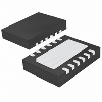
LTC4264IDE#PBF Linear Technology, LTC4264IDE#PBF Datasheet - Page 12

LTC4264IDE#PBF
Manufacturer Part Number
LTC4264IDE#PBF
Description
IC CNTRLR PD INTERFACE 12-DFN
Manufacturer
Linear Technology
Datasheet
1.LTC4264CDEPBF.pdf
(24 pages)
Specifications of LTC4264IDE#PBF
Controller Type
Power over Ethernet Controller (POE)
Interface
IEEE 802.3af
Current - Supply
3mA
Operating Temperature
-40°C ~ 85°C
Mounting Type
Surface Mount
Package / Case
12-DFN
Lead Free Status / RoHS Status
Lead free / RoHS Compliant
Voltage - Supply
-
Available stocks
Company
Part Number
Manufacturer
Quantity
Price
APPLICATIONS INFORMATION
LTC4264
UNDERVOLTAGE LOCKOUT
The IEEE 802.3af specifi cation dictates a maximum turn-
on voltage of 42V and a minimum turn-off voltage of 30V
for the PD. In addition, the PD must maintain large on-off
hysteresis to prevent current-resistance (I-R) drops in the
wiring between the PSE and the PD from causing start-up
oscillation. The LTC4264 incorporates an undervoltage
lockout (UVLO) circuit that monitors line voltage at V
determine when to apply power to the PD load (Figure 7).
Before power is applied to the load, the V
impedance and there is no charge on capacitor C1. When
the input voltage rises above the UVLO turn-on thresh-
old, the LTC4264 removes the classifi cation load current
and turns on the internal power MOSFET. C1 charges up
under LTC4264 inrush current limit control and the V
pin transitions from 0V to V
LTC4264 includes a hysteretic UVLO circuit on V
keeps power applied to the load until the magnitude of the
input voltage falls below the UVLO turn-off threshold. Once
V
disconnects V
is re-enabled. C1 will discharge through the PD circuitry
and the V
12
IN
falls below UVLO turn-off, the internal power MOSFET
OUT
pin will go to a high impedance state.
OUT
from V
IN
and the classifi cation current
IN
PSE
as shown in Figure 3. The
TO
V
LTC4264
IN
INPUT
VOLTAGE
0V TO UVLO*
>UVLO*
*UVLO INCLUDES HYSTERESIS
RISING INPUT THRESHOLD ≅ –38.9V
FALLING INPUT THRESHOLD ≅ –30.6V
Figure 7. LTC4264 Undervoltage Lockout
UNDERVOLTAGE
OUT
LOCKOUT
CIRCUIT
pin is high
IN
POWER MOSFET
IN
that
OUT
LTC4264
to
OFF
ON
INPUT CURRENT LIMIT
IEEE 802.3af specifi es a maximum inrush current and also
specifi es a minimum load capacitor between the GND and
V
the LTC4264 integrates a dual current limit circuit using an
onboard power MOSFET and sense resistor to provide a
complete inrush control circuit without additional external
components.
At turn-on, the LTC4264 will limit the inrush current to
I
voltage in a controlled manner without interference from
the PSE current limit. By keeping the PD current limit below
the PSE current limit, PD power up characteristics are well
controlled and independent of PSE behavior. This ensures
interoperability regardless of PSE output characteristics.
After load capacitor C1 is charged up, the LTC4264 switches
to the high input current limit, I
LTC4264 to deliver up to 35W to the PD load for high power
applications. To maintain compatibility with IEEE 802.3af
power levels, it is necessary for the PD designer to ensure
the PD steady-state power consumption remains below
the limits shown in Table 2. The LTC4264 maintains the
high input current limit until the port voltage drops below
the UVLO turn-off threshold.
LIMIT_LOW
OUT
V
GND
OUT
pins. To control turn-on surge currents in the system
MIN
CURRENT-LIMITED
TURN ON
5µF
, allowing the load capacitor to ramp up to the line
C1
+
4264 F07
LOAD
PD
LIMIT_HIGH
. This allows the
4264f


