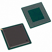
DS3112N Maxim Integrated Products, DS3112N Datasheet - Page 104

DS3112N
Manufacturer Part Number
DS3112N
Description
IC MUX TEMPE T3/E3 IND 256-BGA
Manufacturer
Maxim Integrated Products
Datasheet
1.DS3112.pdf
(133 pages)
Specifications of DS3112N
Controller Type
Framer, Multiplexer
Interface
Parallel/Serial
Voltage - Supply
3.135 V ~ 3.465 V
Current - Supply
150mA
Operating Temperature
-40°C ~ 85°C
Mounting Type
Surface Mount
Package / Case
256-PBGA
Lead Free Status / RoHS Status
Contains lead / RoHS non-compliant
Available stocks
Company
Part Number
Manufacturer
Quantity
Price
Part Number:
DS3112N+
Manufacturer:
DALLAS
Quantity:
20 000
11.2.6 CLAMP
All digital outputs will output data from the boundary scan parallel output while connecting the Bypass
Register between JTDI and JTDO. The outputs will not change during the CLAMP instruction.
11.3 Test Registers
IEEE 1149.1 requires a minimum of two test registers, the bypass register and the boundary scan register.
An optional test register, the Identification register, has been included in the DS3112 design. It is used in
conjunction with the IDCODE instruction and the Test-Logic-Reset state of the TAP controller.
11.3.1 Bypass Register
This is a single one-bit shift register used in conjunction with the BYPASS, CLAMP, and HIGH-Z
instructions that provides a short path between JTDI and JTDO.
11.3.2 Identification Register
The Identification register contains a 32-bit shift register and a 32-bit latched parallel output. This register
is selected during the IDCODE instruction and when the TAP controller is in the Test-Logic-Reset state.
11.3.3
This register contains both a shift register path and a latched parallel output for all control cells and
digital I/O cells and is 196 bits in length.
Table 11-2. Boundary Scan Control Bits
BIT
10
11
12
13
14
15
16
17
18
19
20
21
0
1
2
3
4
5
6
7
8
9
CINT_ENB_N
Boundary Scan Register
CINT_OUT
OUT_ENB
SYMBOL
FRMECU
CINT_IN
T3E3MS
FRDEN
FRCLK
FTDEN
G.747E
FRLOF
FRLOS
FRSOF
CALE
TEST
CWR
CMS
CRD
CIM
CCS
FRD
RST
Control bit
Control bit
PIN
C10
C3
A2
A2
B2
B3
C4
D5
A3
B4
C5
B6
C7
A7
C8
B8
A8
C9
B9
A9
0 = outputs are active
1 = outputs are tri-state (“z”)
I
0 = CINT is a zero (“0”)
1 = CINT is tri-state (“z”)
O (open drain)
I
I
I
I
I
I
I
I
I
I
I
O
O
O
O
O
O
O
I/O OR CONTROL BIT
Table 11-2
DESCRIPTION
104 of 133
shows all the cell bit locations and definitions.
DS3112


