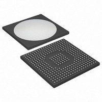
DS31412 Maxim Integrated Products, DS31412 Datasheet - Page 18

DS31412
Manufacturer Part Number
DS31412
Description
IC 12CH DS3/3 FRAMER 349-BGA
Manufacturer
Maxim Integrated Products
Datasheet
1.DS3148.pdf
(89 pages)
Specifications of DS31412
Controller Type
DS3/E3 Framer
Interface
LIU
Voltage - Supply
3.135 V ~ 3.465 V
Current - Supply
960mA
Operating Temperature
-40°C ~ 85°C
Mounting Type
Surface Mount
Package / Case
349-BGA
Lead Free Status / RoHS Status
Lead free / RoHS Compliant
Available stocks
Company
Part Number
Manufacturer
Quantity
Price
7. FUNCTIONAL DESCRIPTION
7.1 Pin Inversions and Force High/Low
Many of the input and output pins can be inverted and some output pins can be forced high or low (TPOS, TNEG,
and RDAT). The inversion logic occurs at the input and output pads but before the JTAG control logic. The output
pins that can be forced high can also be forced low by setting both the force high and invert bits for those pins.
7.2 Transmitter Logic Description
In the normal operating mode, the transmit section adds either DS3 or E3 framing overhead to the payload coming
in on the TDAT input pin, then encodes the framed data in either HDB3 (E3 mode) or B3ZS (DS3 mode) and
outputs the positive and negative pulse signals on TPOS and TNEG along with the transmit clock on TCLK. In line
loopback mode (LLB bit in the
RCLK. In payload loopback mode (PLB bit in the
overhead is added, and TCLK is a buffered version of RCLK. When a transmit alarm indication signal (TAIS) is
generated, an E3 or DS3 AIS signal is generated on TPOS/TNEG independent of the signal being internally
generated. This allows the device to be in diagnostic loopback (DLB) internally and simultaneously send AIS to the
transmit LIU interface. The TAIS is generated when either the TAIS bit in the
there is a loss of transmit clock and the LOTCMC bit in the
of unframed all ones when the TUA1 bit in the
TDAT, RDAT, the BERT (BPLD in BERT payload mode) or the transmit formatter with data from the TOH pin. The
BERT signal in the unframed mode (BUFRM) is not overwritten with the TOH data. The data on TDAT (or RDAT in
PLB mode) can be sent without adding internal overhead by setting the TPT (transmit passthrough) bit in the
T3E3CR1
Figure 7-1. Transmit Data Block Diagram
7.2.1 Transmit Clock
The transmit clock on the TICLK pin is monitored for activity, and, if the clock signal is inactive for several SCLK
cycles, then the loss of transmit clock (LOTC) status is set. The LOTC status is then cleared when the TICLK signal
is active for a few cycles.
The internal transmit clock can be sourced from either the TICLK pin or the RCLK pin, depending on LOTC status,
the LOTCMC control bit (in the
connected to the transmit input clock (TICLK) pin. When LOTC is detected and the LOTCMC bit is set, then the
internal transmit clock is connected to the receive clock (RCLK). Also, if payload loopback (PLB) is selected, then
the internal transmit clock is connected to RCLK. The TCLK output pin is sourced from the internal transmit clock
except in line loopback mode (LLB), where TCLK is always sourced from RCLK.
register. In transmit pass-through mode, data from TOH can still overwrite data from TDAT or RDAT.
TOHEN
TSOF
TDEN
TDAT
TOH
TO Rx BERT
RDAT
BPLD
PLB
MC2
MC1
FORMATTER
register), TPOS, TNEG, and TCLK are buffered versions of RPOS, RNEG, and
E3 G.751
register), and payload loopback (PLB). Normally, the internal transmit clock is
DS3
TPT
MC1
MC2
BERT
register is set. The TOHEN pin overwrites any of the data from
18 of 89
BUFRM
register), payload is sourced from the receiver, framing
MC1
TO RDAT MUX
register is set. The same applies to the generation
HDB3/B3ZS
ENCODER
TO Rx DLB
UNFRAMED ALL
AIS
T3E3CR1
ONES
TAIS
RPOS
RNEG
TUA1
register is set, or when
LLB
TPOS
TNEG


