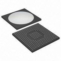
DS31412N Maxim Integrated Products, DS31412N Datasheet - Page 75

DS31412N
Manufacturer Part Number
DS31412N
Description
IC 12CH DS3/3 FRAMER 349-BGA
Manufacturer
Maxim Integrated Products
Datasheet
1.DS3148.pdf
(89 pages)
Specifications of DS31412N
Controller Type
DS3/E3 Framer
Interface
LIU
Voltage - Supply
3.135 V ~ 3.465 V
Current - Supply
960mA
Operating Temperature
-40°C ~ 85°C
Mounting Type
Surface Mount
Package / Case
349-BGA
Lead Free Status / RoHS Status
Lead free / RoHS Compliant
Available stocks
Company
Part Number
Manufacturer
Quantity
Price
11.
All AC timing characteristics are specified with a 50pF capacitive load on the D[7:0] and INT pins, and a 25pF
capacitive load on all other output pins, V
is V
11.1 System Interface Timing
Table 11-A. Data Path Timing
(V
Note 1: E3 mode, nongapped 34.368MHz clock.
Note 2: DS3 mode, nongapped 44.736MHz clock.
Note 3: DS3 mode, gapped 51.84MHz clock.
Note 4: TICLK input to TDAT, TOH, TOHEN, and TSOF inputs; RCLK input to RPOS and RNEG inputs.
Note 5: TICLK input to TDEN (data-enable mode) and TSOF outputs.
Note 6: ROCLK output to RDAT, RDEN (data-enable mode) and RSOF outputs; TCLK output to TPOS and TNEG outputs.
Note 7: RGCLK (gapped clock mode) output to RDAT and RSOF outputs; TDEN/TGCLK (gapped or constant clock mode) output to TSOF
Note 8: TICLK input to TDEN/TGCLK (gapped clock or constant clock mode) outputs; RCLK input to ROCLK output.
Note 9: TMEI, RECU, and RST inputs.
Table 11-B. TCCLK Data Path Timing
(V
Note 10: E3 mode, nongapped 34.368MHz clock.
Note 11: DS3 mode, nongapped 44.736MHz clock.
Note 12: DS3 mode, gapped 51.84MHz clock.
Note 13: TCCLK input to TDAT, TOH, TOHEN, and TSOF inputs.
Note 14: TCCLK input to TDEN/TGCLK (nonclock mode) and TSOF outputs.
Note 15: TCCLK input to TDEN/TGCLK (gapped clock or constant clock mode) outputs.
CLK Clock Period
CLK Clock Duty Cycle
CLK in to DIN Setup Time
CLK in to DIN Hold Time
CLK in to DOUT Delay
CLK out to DOUT Delay
CLK in to CLK Out Delay
Asynchronous Input High, Low Time
Asynchronous Input Period
TCCLK Clock Period
TCCLK Clock Duty Cycle
TCCLK In to DIN Setup Time
TCCLK In to DIN Hold Time
TCCLK In to DOUT Delay
TCCLK In to CLK out Delay
DD
DD
DD
= 3.3V ±5%, T
= 3.3V ±5%, T
/2.
output.
AC TIMING CHARACTERISTICS
PARAMETER
PARAMETER
A
A
= -40°C to +85°C.)
= -40°C to +85°C.)
(Figure
(Figure
IH
= V
SYMBOL
SYMBOL
t8, t9
DD
t2/t1
t2/t1
11-1)
t10
11-2)
t6
t1
t3
t4
t5
t7
t1
t3
t4
t5
t7
and V
75 of 89
IL
(Note 1)
(Note 2)
(Note 3)
(Note 4)
(Note 4)
(Note 5)
(Notes 6, 7)
(Note 8)
(Note 9)
(Note 9)
(Note 10)
(Note 11)
(Note 12)
(Note 13)
(Note 13)
(Note 14)
(Note 15)
= V
SS
CONDITIONS
CONDITIONS
. The voltage threshold for all timing measurements
1000
29.0
22.0
19.0
MIN
MIN
200
5.0
1.0
2.0
2.0
3.0
4.0
2.0
40
29
22
19
40
TYP
29.1
22.4
19.3
TYP
29.1
22.4
19.3
50
50
MAX
MAX
8.0
60
12
10
60
15
15
UNITS
UNITS
ns
ns
ns
ns
ns
ns
ns
ns
ns
ns
ns
ns
ns
%
%


