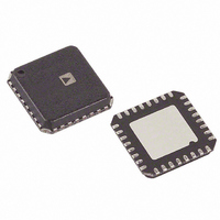
AD9913BCPZ Analog Devices Inc, AD9913BCPZ Datasheet - Page 18

AD9913BCPZ
Manufacturer Part Number
AD9913BCPZ
Description
IC DDS 10BIT DAC 250MSPS 32LFCSP
Manufacturer
Analog Devices Inc
Datasheet
1.AD9913BCPZ.pdf
(32 pages)
Specifications of AD9913BCPZ
Resolution (bits)
10 b
Master Fclk
250MHz
Tuning Word Width (bits)
32 b
Voltage - Supply
1.8 V
Operating Temperature
-40°C ~ 85°C
Mounting Type
Surface Mount
Package / Case
32-LFCSP
Ic Function
Direct Digital Synthesizer
Supply Voltage Range
1.7V To 1.9V
Operating Temperature Range
-40°C To +85°C
Digital Ic Case Style
LFCSP
No. Of Pins
32
Msl
MSL 3 - 168 Hours
Lead Free Status / RoHS Status
Lead free / RoHS Compliant
For Use With
AD9913/PCBZ - BOARD EVAL FOR AD9913
Lead Free Status / RoHS Status
Lead free / RoHS Compliant, Lead free / RoHS Compliant
Available stocks
Company
Part Number
Manufacturer
Quantity
Price
Company:
Part Number:
AD9913BCPZ
Manufacturer:
AD
Quantity:
319
Part Number:
AD9913BCPZ
Manufacturer:
ADI/亚德诺
Quantity:
20 000
AD9913
CLOCK INPUT (REF_CLK)
REF_CLK OVERVIEW
The AD9913 supports a number of options for producing the
internal SYSCLK signal (that is, the DAC sample clock) via the
REF_CLK input pins. The REF_CLK input can be driven
directly from a differential or single-ended source, or it can
accept a crystal connected across the two input pins. There is
also an internal phase-locked loop (PLL) multiplier that can be
independently enabled. The various input configurations are
controlled by means of the control bits in the CFR2 [7:5]
register.
Table 6. Clock Input Mode Configuration
CFR2 [7:5]
000
001
x10
x11
100
101
1
REF_CLK
REF_CLK
CRYSTAL-DRIVEN REF_CLK
When using a crystal at the REF_CLK input, the resonant
frequency should be approximately 25 MHz. Figure 27 shows
the recommended circuit configuration.
DIRECT-DRIVEN REF_CLK
When driving the REF_CLK inputs directly from a signal
source, either single-ended or differential signals can be used.
With a differential signal source, the REF_CLK pins are driven
with complementary signals and ac-coupled with 0.1 μF
capacitors. With a single-ended signal source, either a single-
ended-to-differential conversion can be employed or the
REF_CLK input can be driven single-ended directly. In either
case, 0.1 μF capacitors are used to ac couple both REF_CLK
x = don’t care.
1
1
13
14
Figure 26. Internal Clock Path Functional Block Diagram
XTAL
DIFFERENTIAL/
SINGLE
CMOS
Figure 27. Crystal Connection Diagram
Mode Configuration
Differential Input, PLL Enabled
Differential Input, PLL Disabled (Default)
XTAL Input, PLL Enabled
XTAL Input, PLL Disabled
CMOS Input, PLL Enabled
CMOS Input PLL Disabled
39pF
CFR2[6]
1
0
CFR2[7:6]
00
10
39pF
XTAL
÷2
CFR2[3]
CFR2[14:9]
0
1
13
14
REFCLK
REFCLK
PLL
CFR2[5:0]
CFR2[15]
÷2
0
1
CFR2[5]
1
0
SYSTEM
CLOCK
Rev. A | Page 18 of 32
pins to avoid disturbing the internal dc bias voltage of ~1.35 V.
See Figure 28 for more details.
The REF_CLK input resistance is ~2.7 kΩ differential (~1.35 kΩ
single-ended). Most signal sources have relatively low output
impedances. The REF_CLK input resistance is relatively high,
therefore, its effect on the termination impedance is negligible
and can usually be chosen to be the same as the output imped-
ance of the signal source. The bottom two examples in Figure 28
assume a signal source with a 50 Ω output impedance.
CMOS-DRIVEN REF_CLK
This mode is enabled by writing CFR2 [7] to be true. In this
state, the AD9913 must be driven at Pin 13 with the reference
clock source. Additionally, it is recommended that Pin 14 in
CMOS mode be tied to ground through a 10 kΩ resistor.
PHASE-LOCKED LOOP (PLL) MULTIPLIER
An internal phase-locked loop (PLL) provides users of the
AD9913 the option to use a reference clock frequency that is
lower than the system clock frequency. The PLL supports a wide
range of programmable frequency multiplication factors (1× to
64×). See Table 7 for details on configuring the PLL multipli-
cation factor. The PLL is also equipped with a PLL_LOCK bit.
CFR2 [15:8] and CFR2 [5:1] control the PLL operation. Upon
power-up, the PLL is off. To initialize the PLL, CFR2 [5] must
be cleared and CFR2 [1] must be set. The function of CFR2 [1]
SINGLE-ENDED SOURCE,
SINGLE-ENDED SOURCE,
DIFFERENTIAL SOURCE,
SINGLE-ENDED INPUT
DIFFERENTIAL INPUT
DIFFERENTIAL INPUT
Figure 28. Direct Connection Diagram
DRIVER
Figure 29. CMOS-Driven Diagram
CMOS
LVPECL,
DRIVER
LVDS
10kΩ
OR
BALUN
50Ω
(1:1)
TERMINATION
13
14
REF_CLK
REF_CLK
50Ω
0.1µF
0.1µF
0.1µF
0.1µF
0.1µF
0.1µF
13
14
13
14
13
14
REF_CLK
REF_CLK
REF_CLK
REF_CLK
REF_CLK
REF_CLK


