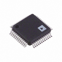
AD9953YSVZ Analog Devices Inc, AD9953YSVZ Datasheet - Page 24

AD9953YSVZ
Manufacturer Part Number
AD9953YSVZ
Description
IC DDS DAC 14BIT 400MSPS 48-TQFP
Manufacturer
Analog Devices Inc
Datasheet
1.AD9953YSVZ.pdf
(32 pages)
Specifications of AD9953YSVZ
Resolution (bits)
14 b
Master Fclk
400MHz
Tuning Word Width (bits)
32 b
Voltage - Supply
1.71 V ~ 1.96 V
Operating Temperature
-40°C ~ 105°C
Mounting Type
Surface Mount
Package / Case
48-TQFP Exposed Pad, 48-eTQFP, 48-HTQFP, 48-VQFP
Data Rate
25Mbps
Rf Ic Case Style
TQFP
No. Of Pins
48
Supply Voltage Range
1.71V To 1.89V, 3.135V To 3.465V
Operating Temperature Range
-40°C To +105°C
Msl
MSL 3 - 168 Hours
Frequency Max
400MHz
Lead Free Status / RoHS Status
Lead free / RoHS Compliant
For Use With
AD9953/PCB - BOARD EVAL FOR AD9953
Lead Free Status / RoHS Status
Lead free / RoHS Compliant, Lead free / RoHS Compliant
Available stocks
Company
Part Number
Manufacturer
Quantity
Price
Company:
Part Number:
AD9953YSVZ
Manufacturer:
Analog Devices Inc
Quantity:
135
Company:
Part Number:
AD9953YSVZ
Manufacturer:
ADI
Quantity:
329
Company:
Part Number:
AD9953YSVZ
Manufacturer:
Analog Devices Inc
Quantity:
10 000
Company:
Part Number:
AD9953YSVZ-REEL7
Manufacturer:
Analog Devices Inc
Quantity:
10 000
AD9953
External Shaped On-Off Keying Mode Operation
The external shaped on-off keying mode is enabled by writing
CFR1<25> to a Logic 1 and writing CFR1<24> to a Logic 0.
When configured for external shaped on-off keying, the
content of the ASFR becomes the scale factor for the data path.
The scale factors are synchronized to SYNC_CLK via the
I/O UPDATE functionality.
Synchronization; Register Updates (I/O UPDATE)
Functionality of the SYNC_CLK and I/O UPDATE
Data into the AD9953 is synchronous to the SYNC_CLK signal
(supplied externally to the user on the SYNC_CLK pin). The
I/O UPDATE pin is sampled on the rising edge of the
SYNC_CLK.
Internally, SYSCLK is fed to a divide-by-4 freque
p
p
s
cl
to
ynchronization of external hardware with the device’s internal
roduce the SYNC_CLK signal. The SYNC_CLK signal is
rovided to the user on the SYNC_CLK pin. This enables
ocks. This is accomplished by forcing any external hardware
obtain its timing from SYNC_CLK. The I/O UPDATE signal
TO CORE LOGIC
SYSCLK
ncy divider to
Figure 21. I/O Synchronization Block Diagram
Q
D
REGISTER
MEMORY
OSK
Rev. A | Page 24 of 32
DETECTION
SYNC_CLK
GATING
÷ 4
LOGIC
EDGE
Q
I/O BUFFER
D
LATCHES
PROFILE<1:0>
coupled with SYNC_CLK is used to transfer internal buffer
contents into the control registers of the device. The combina-
tion of the SYNC_CLK and I/O UPDATE pins provides the
user with constant latency relative to SYSCLK, and also ensures
phase continuity of the analog output signal when a new tuning
word or phase offset value is asserted. Figure 21 demonstrates
an I/O UPDATE timing cycle and synchronization.
Notes for synchronization logic:
1.
2.
The I/O UPDATE signal is edge detected to generate a
single rising edge clock signal that drives the register bank
flops. The I/O UPDATE signal has no constraints on duty
cycle. The minimum low time on I/O UPDATE is one
SYNC_CLK clock cycle.
The I/O UPDATE pin is set up and held around the rising
edge of SYN
time.
Q
D
0
SYNC_CLK
DISABLE
I/O UPDATE
SCLK
SDI
CS
C_CLK and has zero hold time and 4 ns setup


