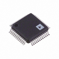
AD9859YSVZ Analog Devices Inc, AD9859YSVZ Datasheet - Page 21

AD9859YSVZ
Manufacturer Part Number
AD9859YSVZ
Description
IC DDS DAC 10BIT 400MSPS 48-TQFP
Manufacturer
Analog Devices Inc
Datasheet
1.AD9859YSVZ-REEL7.pdf
(24 pages)
Specifications of AD9859YSVZ
Resolution (bits)
10 b
Master Fclk
400MHz
Tuning Word Width (bits)
32 b
Voltage - Supply
1.71 V ~ 1.96 V
Operating Temperature
-40°C ~ 105°C
Mounting Type
Surface Mount
Package / Case
48-TQFP Exposed Pad, 48-eTQFP, 48-HTQFP, 48-VQFP
Data Rate
25Mbps
Rf Ic Case Style
TQFP
No. Of Pins
48
Supply Voltage Range
1.71V To 1.89V, 3.135V To 3.465V
Operating Temperature Range
-40°C To +105°C
Msl
MSL 3 - 168 Hours
Frequency Max
400MHz
Lead Free Status / RoHS Status
Lead free / RoHS Compliant
For Use With
AD9859/PCB - BOARD EVAL FOR AD9859
Lead Free Status / Rohs Status
Compliant
Available stocks
Company
Part Number
Manufacturer
Quantity
Price
Company:
Part Number:
AD9859YSVZ
Manufacturer:
Analog Devices Inc
Quantity:
10 000
Company:
Part Number:
AD9859YSVZ-REEL7
Manufacturer:
Analog Devices Inc
Quantity:
10 000
INSTRUCTION BYTE
The instruction byte contains the following information:
Table 7.
MSB
R/ W
R/ W
or write data transfer occurs after the instruction byte write.
Logic High indicates read operation. Logic 0 indicates a write
operation.
X, X—Bits 6 and 5 of the instruction byte are Don’t Cares.
A4, A3, A2, A1, A0—Bits 4, 3, 2, 1, 0 of the instruction byte
determine which register is accessed during the data transfer
portion of the communications cycle.
SERIAL INTERFACE PORT PIN DESCRIPTION
SCLK—Serial Clock. The serial clock pin is used to synchronize
data to and from the AD9859 and to run the internal state
machines. SCLK maximum frequency is 25 MHz.
CSB—Chip Select Bar. CSB is active low input that allows more
than one device on the same serial communications line. The
SDO and SDIO pins go to a high impedance state when this
input is high. If driven high during any communications cycle,
that cycle is suspended until CS
can be tied low in systems that maintain control of SCLK.
SDIO—Serial Data I/O. Data is always written to the AD9859
on this pin. However, this pin can be used as a bidirectional
data line. Bit 9 of Register Address 0x00 controls the
configuration of this pin. The default is Logic 0, which
configures the SDIO pin as bidirectional.
SDO—Serial Data Out. Data is read from this pin for protocols
that use separate lines for transmitting and receiving data. In
the case where the AD9859 operates in a single bidirectional
I/O mode, this pin does not output data and is set to a high
impedance state.
IOSYNC—It synchronizes the I/O port state machines without
affecting the addressable register’s contents. An active high
input on the IOSYNC pin causes the current communication
cycle to abort. After IOSYNC returns low (Logic 0), another
communication cycle may begin, starting with the instruction
byte write.
MSB/LSB TRANSFERS
The AD9859 serial port can support both most significant bit
(MSB) first or least significant bit (LSB) first data formats. This
functionality is controlled by the Control Register 0x00 <8> bit.
The default value of Control Register 0x00 <8> is low (MSB
first). When Control Register 0x00 <8> is set high, the AD9859
serial port is in LSB first format. The instruction byte must be
—Bit 7 of the instruction byte determines whether a read
D6
X
is reactivated low. Chip select
D5
X
D4
A4
Rev. A | Page 21 of 24
D3
A3
written in the format indicated by Control Register 0x00 <8>. If
the AD9859 is in LSB first mode, the instruction byte must be
written from least significant bit to most significant bit.
For MSB first operation, the serial port controller generates the
most significant byte (of the specified register) address first
followed by the next lesser significant byte addresses until the
I/O operation is complete. All data written to (read from) the
AD9859 must be (is) in MSB first order. If the LSB mode is
active, the serial port controller generates the least significant
byte address first followed by the next greater significant byte
addresses until the I/O operation is complete. All data written to
(read from) the AD9859 must be (is) in LSB first order.
Example Operation
To write the amplitude scale factor register in MSB first format,
apply an instruction byte of 0x02 [serial address is 00010(b)].
From this instruction, the internal controller knows to use the
first byte as the most significant byte. The first two bits are
recorded as the auto ramp rate speed control bits, and the next
six bits are the most significant bits of the amplitude scale
factor. The second byte is applied as the eight less significant
bits of the amplitude scale factor ASF<7:0>.
To write the amplitude scale factor register in LSB first format,
assuming the control register has already been set for LSB first
format, apply an instruction byte of 0x40. From this instruction,
the internal controller knows to use the first byte as the least
significant byte of the amplitude scale factor ASF<0:7>. The
second byte is split into the first six bits ASF<8:13> and the last
two provide the auto-ramp rate speed control bits ARRSC<0:1>.
Power-Down Functions of the AD9859
The AD9859 supports an externally controlled or hardware
power-down feature as well as the more common software
programmable power-down bits found in previous Analog Devices,
Inc., DDS products.
The software control power-down allows the DAC, PLL, input
clock circuitry, and digital logic to be individually powered
down via unique control bits (CFR1<7:4>). With the exception
of CFR1<6>, these bits are not active when the externally
controlled power-down pin (PWRDWNCTL) is high. External
power-down control is supported on the AD9859 via the
PWRDWNCTL input pin. When the PWRDWNCTL input pin
is high, the AD9859 enters a power-down mode based on the
CFR1<3> bit. When the PWRDWNCTL input pin is low, the
external power-down control is inactive.
D2
A2
D1
A1
LSB
A0
AD9859


