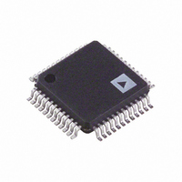
AD9954YSVZ Analog Devices Inc, AD9954YSVZ Datasheet - Page 21

AD9954YSVZ
Manufacturer Part Number
AD9954YSVZ
Description
IC DDS DAC 14BIT 1.8V 48-TQFP
Manufacturer
Analog Devices Inc
Datasheet
1.AD9954YSVZ-REEL7.pdf
(40 pages)
Specifications of AD9954YSVZ
Resolution (bits)
14 b
Master Fclk
400MHz
Tuning Word Width (bits)
32 b
Voltage - Supply
1.71 V ~ 1.96 V
Operating Temperature
-40°C ~ 105°C
Mounting Type
Surface Mount
Package / Case
48-TQFP Exposed Pad, 48-eTQFP, 48-HTQFP, 48-VQFP
Data Rate
25Mbps
Rf Ic Case Style
TQFP
No. Of Pins
48
Supply Voltage Range
1.71V To 1.89V, 3.135V To 3.465V
Operating Temperature Range
-40°C To +105°C
Msl
MSL 3 - 168 Hours
Termination Type
SMD
Rohs Compliant
Yes
Filter Terminals
SMD
Lead Free Status / RoHS Status
Lead free / RoHS Compliant
For Use With
AD9954/PCBZ - BOARD EVAL FOR 9954
Lead Free Status / RoHS Status
Lead free / RoHS Compliant, Lead free / RoHS Compliant
Available stocks
Company
Part Number
Manufacturer
Quantity
Price
Company:
Part Number:
AD9954YSVZ
Manufacturer:
ADI
Quantity:
210
Company:
Part Number:
AD9954YSVZ
Manufacturer:
Analog Devices Inc
Quantity:
10 000
Part Number:
AD9954YSVZ
Manufacturer:
ADI/亚德诺
Quantity:
20 000
Company:
Part Number:
AD9954YSVZ-REEL7
Manufacturer:
UBR
Quantity:
6 000
Company:
Part Number:
AD9954YSVZ-REEL7
Manufacturer:
Analog Devices Inc
Quantity:
10 000
SYNCHRONIZATION—REGISTER UPDATES (I/O
UPDATE)
Functionality of the SYNC_CLK and I/O UPDATE
Data into the AD9954 is synchronous to the SYNC_CLK
signal (supplied externally to the user on the SYNC_CLK pin).
The I/O UPDATE pin is sampled on the rising edge of the
SYNC_CLK.
Internally, SYSCLK is fed to a divide-by-four frequency divider
to produce the SYNC_CLK signal. The SYNC_CLK signal is
made available to the system on the SYNC_CLK pin. This
enables synchronization of external hardware with the device’s
internal clocks. This is accomplished by providing the SYNC_CLK
signal as an output that external hardware can then use to
synchronize against.
I/O BUFFERS
I/O UPDATE
REGISTERS
SYNC_CLK
SYSCLK
DATA IN
DATA IN
THE DEVICE REGISTERS AN I/O UPDATE AT POINT A. THE DATA IS TRANSFERRED FROM
THE ASYNCHRONOUSLY LOADED I/O BUFFERS AT POINT B.
N
N – 1
TO CORE LOGIC
A
SYSCLK
Figure 24. I/O Synchronization Timing Diagram
Figure 23. I/O Synchronization Block Diagram
B
Q
D
REGISTER
MEMORY
OSK
N + 1
Rev. B | Page 21 of 40
DETECTION
SYNC_CLK
GATING
LOGIC
÷4
EDGE
Q
I/O BUFFER
D
LATCHES
PS<1:0>
The I/O update signal coupled with SYNC_CLK is used to
transfer internal buffer contents into the control registers. The
combination of the SYNC_CLK pin and the I/O UPDATE pin
provides the user with constant latency relative to SYSCLK and
ensures phase continuity of the analog output signal when a
new tuning word or phase offset value is asserted.
Figure 23 and Figure 24 demonstrate an I/O update timing
cycle and synchronization.
Synchronization logic notes include the following:
The I/O update signal is edge detected to generate a single-
The I/O UPDATE pin is set up and held around the rising
cycle clock signal that drives the register bank flops. The I/O
update signal has no constraints on duty cycle. The minimum
low time on I/O update is one SYNC_CLK clock cycle.
edge of SYNC_CLK. Setup and hold time specifications can
be found in Table 2.
N
Q
D
0
SYNC_CLK
DISABLE
I/O UPDATE
SCLK
SDIO
CS
N + 2
N + 1
AD9954


