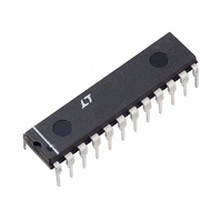
LT1134ACN#PBF Linear Technology, LT1134ACN#PBF Datasheet - Page 7

LT1134ACN#PBF
Manufacturer Part Number
LT1134ACN#PBF
Description
IC 4DRV/4RCV RS232 5V 24-DIP
Manufacturer
Linear Technology
Type
Transceiverr
Datasheet
1.LT1134ACSWPBF.pdf
(12 pages)
Specifications of LT1134ACN#PBF
Number Of Drivers/receivers
4/4
Protocol
RS232
Voltage - Supply
4.5 V ~ 5.5 V
Mounting Type
Through Hole
Package / Case
24-DIP (0.300", 7.62mm)
Data Rate
250Kbps
Interface Circuit Standard 1
RS-232
Number Of Receivers
4
Number Of Transmitters
4
Number Of Transceivers
4
Data Transmission Topology
Point-to-Point
Receiver Signal Type
Single-Ended
Transmitter Signal Type
Single-Ended
Single Supply Voltage (typ)
5/12V
Dual Supply Voltage (typ)
Not RequiredV
Dual Supply Voltage (min)
Not RequiredV
Dual Supply Voltage (max)
Not RequiredV
Supply Current
25mA
Power Supply Requirement
Single
Operating Temp Range
0C to 70C
Operating Temperature Classification
Commercial
Mounting
Through Hole
Pin Count
24
Package Type
PDIP N
Lead Free Status / RoHS Status
Lead free / RoHS Compliant
Available stocks
Company
Part Number
Manufacturer
Quantity
Price
TYPICAL PERFOR
PI FU CTIO S
V
the shutdown mode. This pin should be decoupled with a
0.1 F ceramic capacitor close to the package pin. Insuffi-
cient supply bypassing can result in low output drive levels
and erratic charge pump operation.
GND: Ground Pin.
ON/OFF: Control the operation mode of the device and is
TTL/CMOS compatible. A logic low puts the device in the
shutdown mode which reduces input supply curent to zero
and places all of the drivers and receivers in high imped-
ance state. A logic high fully enables the transceiver.
DRIVER DISABLE: This pin provides an alternate control
for the charge pump and RS232 drivers. A logic high on
this pin shuts down the charge pump and places all drivers
CC
U
OUTPUT HIGH
: 5V Input Supply Pin. Supply current drops to zero in
OUTPUT LOW
ON/OFF PIN
DRIVER
DRIVER
R
R
L
L
= 3k
= 3k
U
– 10
– 5
10
30
25
20
15
10
5
0
0
5
–55
Driver Short-Circuit Current
Shutdown to Driver Output
–25
U
0
TEMPERATURE (°C)
W
25
A
50
U
CE
75
ISC
ISC
LT1137A • TPC10
C
+
–
100
LT1137A • TPC12
HARA TERISTICS
125
C
DRIVER OUTPUT
DRIVER OUTPUT
in a high impedance state. Receivers remain active under
these conditions. Floating the DRIVER DISABLE pin or
driving it to a logic low level fully enables the transceiver.
A logic low on the ON/OFF pin supersedes the state of the
DRIVER DISABLE pin. Supply current drops to 4mA when
in driver disable mode.
V
1.5V. This pin requires an external charge storage capaci-
tor C 1.0 F, tied to ground or V
tors may be used to reduce supply ripple. With multiple
transceivers, the V
common capacitors. For large numbers of transceivers,
increasing the size of the shared common storage capaci-
tors is recommended to reduce ripple.
+
C
: Positive Supply Output (RS232 Drivers). V
L
= 2500pF
R
R
L
INPUT
L
= 3k
= 3k
50
40
30
20
10
0
–55
Driver Output Waveforms
Receiver Short-Circuit Current
LT1130A/LT1140A Series
–25
0
+
TEMPERATURE (°C)
ISC
and V
+
25
ISC
–
50
–
pins may be paralleled into
75
CC
LT1137A • TPC11
100
. Larger value capaci-
LT1137A • TPC13
125
+
2V
CC
7
–


