DS26LS32CM/NOPB National Semiconductor, DS26LS32CM/NOPB Datasheet - Page 3
DS26LS32CM/NOPB
Manufacturer Part Number
DS26LS32CM/NOPB
Description
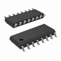
IC LINE RCVR QUAD DIFF 16-SOIC
Manufacturer
National Semiconductor
Type
Receiverr
Datasheet
1.DS26LS32ACMNOPB.pdf
(8 pages)
Specifications of DS26LS32CM/NOPB
Number Of Drivers/receivers
0/4
Protocol
RS422, RS423
Voltage - Supply
4.5 V ~ 5.5 V
Mounting Type
Surface Mount
Package / Case
16-SOIC (3.9mm Width)
Termination Type
SMD
Driver Case Style
NSOIC
No. Of Pins
16
Operating Temperature Range
0°C To +70°C
Supply Voltage Min
4.75V
Output Current Max
20µA
No. Of Driver/receivers
0/4
Rohs Compliant
Yes
Lead Free Status / RoHS Status
Lead free / RoHS Compliant
Other names
*DS26LS32CM
*DS26LS32CM/NOPB
DS26LS32CM
*DS26LS32CM/NOPB
DS26LS32CM
Available stocks
Company
Part Number
Manufacturer
Quantity
Price
Company:

Part Number:
DS26LS32CM/NOPB
Manufacturer:
NS
Quantity:
1 232
Part Number:
DS26LS32CM/NOPB
Manufacturer:
NS/国半
Quantity:
20 000


Symbol
V
R
I
V
V
V
V
V
I
I
I
I
I
I
V
IN
O
IL
IH
SC
CC
I
TH
IN
OH
OL
IL
IH
I
HYST
Absolute Maximum Ratings
If Military/Aerospace specified devices are required,
please contact the National Semiconductor Sales Office/
Distributors for availability and specifications.
Electrical Characteristics
over the operating temperature range unless otherwise specified
Note 3: “Absolute Maximum Ratings” are those values beyond which the safety of the device cannot be guaranteed. They are not meant to imply that the device
should be operated at these limits. The table of “Electrical Characteristics” provides conditions for actual device operation.
Note 4: All currents into device pins are shown as positive, all currents out of device pins are shown as negative, all voltages are referenced to ground, unless
otherwise specified. All values shown as max or min are so classified on absolute value basis.
Note 5: All typical values are V
Note 6: Only one output at a time should be shorted.
Supply Voltage
Common-Mode Range
Differential Input Voltage
Enable Voltage
Output Sink Current
Maximum Power Dissipation (Note 1) at 25˚C
Storage Temperature Range
Lead Temperature (Soldering, 4
seconds)
Cavity Package
Molded Dip Package
SO Package DS26LS32
DS26LS32A
Differential Input
Voltage
Input Resistance
Input Current (Under
Test)
Output High Voltage
Output Low Voltage
Enable Low Voltage
Enable High Voltage
Enable Clamp
Voltage
OFF-State (High
Impedance) Output
Current
Enable Low Current
Enable High Current
Output Short-Circuit
Current
Power Supply
Current
Input High Current
Input Hysteresis
Parameter
CC
= 5V, T
V
or V
−15V ≤ V
V
V
V
V
V
V
V
V
V
V
V
V
Outputs Disabled
V
T
V
A
A
OUT
CC
ENABLE
CC
ENABLE
CC
IN
IN
CC
IN
CM
IN
IN
CC
O
= 25˚C.
= 25˚C, V
= 0.4V
= 2.7V
= 5.5V
OL
= 0V, V
= 15V, Other Input −15V ≤ V
= −15V, Other Input −15V ≤ V
= MIN, ∆V
= Min, ∆V
= Min, I
= Max, All V
= 0V
= Max
= V
= 0.8V, I
= 0.8V
OH
CM
(Notes 4, 5, 6)
CC
IN
≤ +15V (One Input AC GND)
CC
(Note 3)
IN
= −18 mA
IN
= Max, ∆V
1433 mW
1362 mW
1002 mW
1051 mW
= 5V,
DS26LS32, DS26LS32A, −7V ≤ V
DS26LS33, DS26LS33A, −15V ≤ V
−65˚C to
= −1V,
IN
= 1V,
OH
+165˚C
50 mA
= GND,
260˚C
±
±
= −440 µA
25V
25V
7V
7V
Conditions
IN
= 1V
3
IN
Operating Conditions
Note 1: Derate cavity package 9.6 mW/˚C above 25˚C; derate molded DIP
package 10.9 mW/˚C above 25˚C.
Note 2: Derate SO Package 8.01 mW/˚C for DS26LS32
IN
Supply Voltage, (V
Temperature, (T
Commercial
Military
I
I
V
V
DS26LS32, DS26LS32A
DS26LS33, DS26LS33A
DS26LS32, DS26S32A
DS26LS33, DS26LS33A
8.41 mW/˚C for DS26LS32A
≤ +15V
OL
OL
≤ +15V
O
O
DS26LS32M, DS26LS33M
(MIL)
DS26LS32C
DS26LS32AC
(COML)
DS26LS32M, DS26LS33M
(MIL)
DS26LS32C
DS26LS32AC
(COML)
= 2.4V
= 0.4V
= 4 mA
= 8 mA
CM
A
CM
)
CC
≤ +7V
+15V
)
−0.2
−0.5
Min
−15
6.0
2.7
2.5
2.0
4.75
Min
−55
4.5
0
±
±
Typ
100
200
8.5
4.2
4.2
0.07
0.14
52
57
+125
Max
5.25
+70
5.5
−0.36
Max
−2.8
0.45
−1.5
−20
−85
100
www.national.com
0.2
0.5
2.3
0.4
0.8
20
20
70
80
Units
˚C
˚C
V
V
Units
mA
mA
mA
mA
mA
mA
mV
mV
kΩ
µA
µA
µA
µA
V
V
V
V
V
V
V
V
V
Related parts for DS26LS32CM/NOPB
Image
Part Number
Description
Manufacturer
Datasheet
Request
R

Part Number:
Description:
Quad Differential Line Receivers
Manufacturer:
National Semiconductor
Datasheet:
Part Number:
Description:
National Semiconductor [8-Bit D/A Converter]
Manufacturer:
National Semiconductor
Datasheet:
Part Number:
Description:
National Semiconductor [Media Coprocessor]
Manufacturer:
National Semiconductor
Datasheet:
Part Number:
Description:
Digitally Controlled Tone and Volume Circuit with Stereo Audio Power Amplifier, Microphone Preamp Stage and National 3D Sound
Manufacturer:
National Semiconductor
Datasheet:
Part Number:
Description:
Digitally Controlled Tone and Volume Circuit with Stereo Audio Power Amplifier, Microphone Preamp Stage and National 3D Sound
Manufacturer:
National Semiconductor
Datasheet:
Part Number:
Description:
AC97 Rev 2 Codec with Sample Rate Conversion and National 3D Sound
Manufacturer:
National Semiconductor
Part Number:
Description:
Manufacturer:
National Semiconductor
Datasheet:
Part Number:
Description:
Manufacturer:
National Semiconductor
Datasheet:
Part Number:
Description:
General Purpose, Low Voltage, Low Power, Rail-to-Rail Output Operational Amplifiers
Manufacturer:
National Semiconductor
Datasheet:
Part Number:
Description:
8-bit 20 MSPS flash A/D converter.
Manufacturer:
National Semiconductor
Datasheet:
Part Number:
Description:
Low Noise Quad Operational Amplifier
Manufacturer:
National Semiconductor
Datasheet:
Part Number:
Description:
Quad Differential Line Receivers
Manufacturer:
National Semiconductor
Datasheet:
Part Number:
Description:
Quad High Speed Trapezoidal? Bus Transceiver
Manufacturer:
National Semiconductor
Datasheet:
Part Number:
Description:
Dual Line Receiver
Manufacturer:
National Semiconductor
Datasheet: