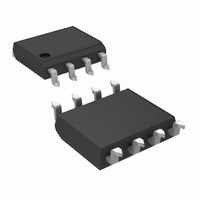
DS89C21TM/NOPB National Semiconductor, DS89C21TM/NOPB Datasheet - Page 3

DS89C21TM/NOPB
Manufacturer Part Number
DS89C21TM/NOPB
Description
IC LINE DRV/RCVR DIFF PAIR 8SOIC
Manufacturer
National Semiconductor
Type
Transceiverr
Datasheet
1.DS89C21TMNOPB.pdf
(6 pages)
Specifications of DS89C21TM/NOPB
Number Of Drivers/receivers
1/1
Protocol
RS422
Voltage - Supply
4.5 V ~ 5.5 V
Mounting Type
Surface Mount
Package / Case
8-SOIC (3.9mm Width)
Number Of Receivers
1
Receiver Signal Type
Differential
Interface Type
EIA/TIA-422-A, RS-422, V.11
Operating Supply Voltage
5 V
Maximum Operating Temperature
+ 85 C
Minimum Operating Temperature
- 40 C
Data Rate
20 Mbps
Mounting Style
SMD/SMT
Supply Current
12 mA
Lead Free Status / RoHS Status
Lead free / RoHS Compliant
Other names
*DS89C21TM
*DS89C21TM/NOPB
DS89C21TM
*DS89C21TM/NOPB
DS89C21TM
Available stocks
Company
Part Number
Manufacturer
Quantity
Price
Company:
Part Number:
DS89C21TM/NOPB
Manufacturer:
National Semiconductor
Quantity:
1 958
Company:
Part Number:
DS89C21TM/NOPB
Manufacturer:
VISHAY
Quantity:
5 485
Part Number:
DS89C21TM/NOPB
Manufacturer:
TI/德州仪器
Quantity:
20 000
RECEIVER CHARACTERISTICS
V
V
I
DRIVER AND RECEIVER CHARACTERISTICS
I
DIFFERENTIAL DRIVER CHARACTERISTICS
t
t
t
t
t
RECEIVER CHARACTERISTICS
t
t
t
t
t
OSR
CC
PLHD
PHLD
SKD
TLH
THL
PLH
PHL
SK
r
f
Symbol
OH
OL
Symbol
Electrical Characteristics
Over recommended supply voltage and operating temperature ranges, unless otherwise specified.
Switching Characteristics
Over recommended supply voltage and operating temperature ranges, unless otherwise specified.
Note 1: “Absolute Maximum Ratings” are those values beyond which the safety of the device cannot be guaranteed. They are not meant to imply that the devices
should be operated at these limits. The tables of “Electrical Characteristics” specify conditions for device operation.
Note 2: Current into device pins is defined as positive. Current out of device pins is defined as negative. All voltages are referenced to ground unless otherwise
specified.
Note 3: All typicals are given for V
Note 4: f = 1 MHz, t
Note 5: ESD Rating: HBM (1.5 kΩ, 100 pF) all pins ≥ 2000V.
EIAJ (0Ω, 200 pF) ≥ 250V
Parameter Measurement Information
Output HIGH Voltage
Output LOW Voltage
Output Short Circuit Current
Supply Current
Propagation Delay LOW to HIGH
Propagation Delay HIGH to LOW
Skew, |t
Transition Time LOW to HIGH
Transition Time HIGH to LOW
Propagation Delay LOW to HIGH
Propagation Delay HIGH to LOW
Skew, |t
Rise Time
Fall Time
r
and t
PLHD
PLH
f
–t
≤ 6 ns.
Parameter
Parameter
–t
PHL
PHLD
|
CC
|
= 5.0V and T
A
(Notes 2, 3) (Continued)
= 25˚C.
(Note 3)
FIGURE 1. V
I
I
V
No Load
R
C
C
V
V
OH
OL
L
L
L
DIFF
CM
OUT
= 100Ω
= 50 pF
= 50 pF
= −6 mA
= +6 mA, V
= 0V
= 0V
= 2.5V
OD
and V
3
DIFF
Conditions
Conditions
(Figures 2, 3)
(Figures 2, 4)
(Figures 5, 6)
(Figure 7)
OC
= −1V
V
V
DI = V
DI = 2.4V or 0.5V
Test Circuit
DIFF
DIFF
= +1V
= OPEN
CC
or GND
01175302
V
Pin
RO
CC
Min
2
2
6
6
Min
−25
3.8
3.8
17.5
Typ
4.9
4.5
0.4
2.2
2.1
0.5
2.5
2.1
18
0.08
Typ
−85
4.9
4.9
3.0
3.8
Max
2.0
4.0
−150
10
10
30
30
Max
www.national.com
9
9
9
9
0.3
12
6
Units
Units
mA
mA
mA
ns
ns
ns
ns
ns
ns
ns
ns
ns
ns
V
V
V


