DP83848TSQ/NOPB National Semiconductor, DP83848TSQ/NOPB Datasheet
DP83848TSQ/NOPB
Specifications of DP83848TSQ/NOPB
Available stocks


Related parts for DP83848TSQ/NOPB

DP83848TSQ/NOPB Summary of contents
Page 1
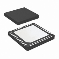
... DP83848H is offered in a small 6mm x 6mm LLP 40-pin package. System Diagram MII/RMII MPU/CPU ® PHYTER is a registered trademark of National Semiconductor Corporation. © 2008 National Semiconductor Corporation ® Mini - Extreme Single 10/100 Ethernet Features • Low-power 3.3V, 0.18 m CMOS technology • Auto-MDIX for 10/100 Mb/s • ...
Page 2
TX_DATA TX_CLK 10BASE-T & 100BASE-TX Transmit Block DAC Auto-MDIX www.national.com MII/RMII SERIAL MANAGEMENT MII/RMII INTERFACE MII Registers Auto-Negotiation State Machine Clock Generation TD± RD± REFERENCE CLOCK Figure 1. DP83848H Functional Block Diagram 2 RX_CLK RX_DATA 10BASE-T & 100BASE-TX Receive Block ...
Page 3
Pin Descriptions . . . . . . . . . . . . . . . . . . . . . . . . . . . . . . . . . . . . . ...
Page 4
Decoder . . . . . . . . . . . . . . . . . . . . . . . . . . . . . . . . . . . . . ...
Page 5
Mb/s MII Receive Timing . . . . . . . . . . . . . . . . . . . . . . . . . . . . . . . . . . ...
Page 6
Figure 1. DP83848H Functional Block Diagram . . . . . . . . . . . . . . . . . . . . . . . . . . . . . . . . . . ...
Page 7
Table 1. Auto-Negotiation Modes . . . . . . . . . . . . . . . . . . . . . . . . . . . . . . . . . . . . ...
Page 8
Pin Layout IOVDD33 TX_CLK TX_EN TXD_0 TXD_1 TXD_2 TXD_3 RESERVED RESERVED RESERVED Note: Die Attached Pad (DAP) provides thermal dissipation, connection to GND plane recommended. www.national.com DP83848H DAP 10 Top View ...
Page 9
Pin Descriptions The DP83848H pins are classified into the following inter- face categories (each interface is described in the sections that follow): — Serial Management Interface — MAC Data Interface — Clock Interface — LED Interface — Reset — ...
Page 10
Signal Name Type RX_ER RXD_0 RXD_1 RXD_2 RXD_3 CRS/CRS_DV COL 1.3 Clock Interface Signal Name Type X1 X2 www.national.com Pin # 34 MII RECEIVE ERROR: Asserted high synchronously ...
Page 11
Signal Name Type 25MHz_OUT O 1.4 LED Interface See Table 3 for LED Mode Selection. Signal Name Type LED_LINK 1.5 Reset Signal Name Type RESET_N I, PU 1.6 Strap Options DP83848H uses many functional pins as strap ...
Page 12
Signal Name Type AN0 (LED_LINK MII_MODE (RX_DV LED_CFG (CRS/CRS_DV MDIX_EN (RX_ER www.national.com Pin # Description 22 This input pin controls the advertised operating mode of the DP83848H according ...
Page 13
Mb/s and 100 Mb/s PMD Interface Signal Name Type TD-, TD+ I/O RD-, RD+ I/O 1.8 Special Connections Signal Name Type RBIAS I PFBOUT O PFBIN1 I PFBIN2 RESERVED I/O 1.9 Power Supply Pins Signal Name IOVDD33 IOGND ...
Page 14
Package Pin Assignments NSQAu040 Pin Name Pin # 1 IO_VDD 2 TX_CLK 3 TX_EN 4 TXD_0 5 TXD_1 6 TXD_2 7 TXD_3 8 RESERVED 9 RESERVED 10 RESERVED 11 RD- 12 RD+ 13 AGND ...
Page 15
Configuration This section includes information on the various configura- tion options available with the DP83848H. The configura- tion options described below include: — Auto-Negotiation — PHY Address and LED — Half Duplex vs. Full Duplex — Isolate mode — ...
Page 16
Auto-Negotiation Parallel Detection The DP83848H supports the Parallel Detection function as defined in the IEEE 802.3u specification. Parallel Detection requires both the 10 Mb/s and 100 Mb/s receivers to moni- tor the receive signal and report link status to ...
Page 17
PHY Address The 5 PHY address inputs pins are shared with the RXD[3:0] pins and COL pin as shown below. Table 2. PHY Address Mapping Pin # PHYAD Function 35 PHYAD0 36 PHYAD1 37 PHYAD2 38 PHYAD3 39 PHYAD4 ...
Page 18
LED Interface The DP83848H supports a configurable Light Emitting Diode (LED) pin for configuring the link. The PHY Control Register (PHYCR) for the LED can also be selected through address 19h, bit [5]. See Table 3 for LED Mode ...
Page 19
Half Duplex vs. Full Duplex The DP83848H supports both half and full duplex opera- tion at both 10 Mb/s and 100 Mb/s speeds. Half-duplex relies on the CSMA/CD protocol to handle col- lisions and network access. In Half-Duplex mode, ...
Page 20
Functional Description The DP83848H supports two modes of operation using the MII interface pins. The options are defined in the following sections and include: — MII Mode — RMII Mode The modes of operation can be selected by strap ...
Page 21
To tolerate potential frequency differences between the 50 MHz reference clock and the recovered receive clock, the receive RMII function includes a programmable elasticity buffer. The elasticity buffer is programmable to minimize propagation delay based on expected packet size and ...
Page 22
MDC Z MDIO (STA) MDIO (PHY Opcode PHY Address Idle Start (Read) (PHYAD = 0Ch) MDC Z MDIO (STA ...
Page 23
Architecture This section describes the operations within each trans- ceiver module, 100BASE-TX and 10BASE-T. Each opera- tion consists of several functional blocks and described in the following: — 100BASE-TX Transmitter — 100BASE-TX Receiver — 10BASE-T Transceiver Module 4.1 100BASE-TX ...
Page 24
DATA CODES IDLE AND CONTROL CODES INVALID CODES Note: Control ...
Page 25
Code-group Encoding and Injection The code-group encoder converts 4-bit (4B) nibble data generated by the MAC into 5-bit (5B) code-groups for transmission. This conversion is required to allow control data to be combined with packet data code-groups. Refer to ...
Page 26
RX_DV/CRS RX_CLK RX_DATA VALID SSD DETECT www.national.com RXD[3:0] / RX_ER 4B/5B DECODER SERIAL TO PARALLEL CODE GROUP ALIGNMENT DESCRAMBLER NRZI TO NRZ DECODER MLT-3 TO BINARY DECODER DIGITAL SIGNAL PROCESSOR ANALOG FRONT END RD Figure 7. 100BASE-TX Receive Block Diagram ...
Page 27
Digital Adaptive Equalization and Gain Control When transmitting data at high speeds over copper twisted pair cable, frequency dependent attenuation becomes a concern. In high-speed twisted pair signalling, the frequency content of the transmitted signal can vary greatly during ...
Page 28
Base Line Wander Compensation The DP83848H is completely ANSI TP-PMD compliant and includes Base Line Wander (BLW) compensation. The BLW compensation block can successfully recover the TP- PMD defined “killer” pattern. BLW can generally be defined as the change ...
Page 29
Descrambler A serial descrambler is used to de-scramble the received NRZ data. The descrambler has to generate an identical data scrambling sequence (N) in order to recover the orig- inal unscrambled data (UD) from the scrambled data (SD) as ...
Page 30
Smart Squelch The smart squelch is responsible for determining when valid data is present on the differential receive inputs. The DP83848H implements an intelligent receive squelch to ensure that impulse noise on the receive inputs will not be mistaken ...
Page 31
Jabber Function The jabber function monitors the DP83848H's output and disables the transmitter if it attempts to transmit a packet of longer than legal size. A jabber timer monitors the transmitter and disables the transmission if the transmitter is ...
Page 32
Design Guidelines 5.1 TPI Network Circuit Figure 11 shows the recommended circuit for a 10/100 Mb/s twisted pair interface. To the right is a partial list of recommended transformers important that the user realize that variations with ...
Page 33
ESD Protection Typically, ESD precautions are predominantly in effect when handling the devices or board before being installed in a system. In those cases, strict handling procedures need be implemented during the manufacturing process to greatly reduce the occurrences ...
Page 34
Parameter Min Frequency Frequency Tolerance Frequency Stability Rise / Fall Time Jitter Jitter Symmetry 40% 1. This limit is provided as a guideline for component selection and not guaranteed by production testing. Refer to AN-1548, “PHYTER 100 Base-TX Reference Clock ...
Page 35
Power Feedback Circuit To ensure correct operation for the DP83848H, parallel caps with values (Tantalum) and 0.1 F should be placed close to pin 19 (PFBOUT) of the device. Pin 16 (PFBIN1) and pin 30 (PFBIN2) ...
Page 36
Register Block Offset Access Hex Decimal 00h 0 RW 01h 1 RO 02h 2 RO 03h 3 RO 04h 4 RW 05h 5 RW 05h 5 RW 06h 6 RW 07h 7 RW 08h-Fh 8-15 RW 10h 16 RO ...
Page 37
37 www.national.com ...
Page 38
www.national.com 38 ...
Page 39
Register Definition In the register definitions under the ‘Default’ heading, the following definitions hold true: — RW=Read Write access SC — =Register sets on event occurrence and Self-Clears when event ends — RW/SC =Read Write access/Self Clearing bit — ...
Page 40
Basic Mode Control Register (BMCR) Table 12. Basic Mode Control Register (BMCR), address 0x00 Bit Bit Name 15 Reset 14 Loopback 13 Speed Selection 12 Auto-Negotiation Enable 11 Power Down 10 Isolate 9 Restart Auto- Negotiation 8 Duplex Mode ...
Page 41
Table 12. Basic Mode Control Register (BMCR), address 0x00 (Continued) Bit Bit Name Default 7 Collision Test 0, RW 6:0 RESERVED 0, RO Description Collision Test Collision test enabled Normal operation. When set, this bit will ...
Page 42
Basic Mode Status Register (BMSR) Table 13. Basic Mode Status Register (BMSR), address 0x01 Bit Bit Name 15 100BASE-T4 14 100BASE-TX Full Duplex 13 100BASE-TX Half Duplex 12 10BASE-T Full Duplex 11 10BASE-T Half Duplex 10:7 RESERVED 6 MF ...
Page 43
The PHY Identifier Registers #1 and #2 together form a unique identifier for the DP83848H. The Identifier consists of a concatenation of the Organizationally Unique Identifier (OUI), the vendor's model number and the model revision num- ber. A PHY may ...
Page 44
Table 16. Negotiation Advertisement Register (ANAR), address 0x04 (Continued) Bit Bit Name 11 ASM_DIR 10 PAUSE TX_FD 10_FD 5 10 4:0 Selector www.national.com Default 0, RW Asymmetric PAUSE Support for Full Duplex Links: The ...
Page 45
Auto-Negotiation Link Partner Ability Register (ANLPAR) (BASE Page) This register contains the advertised abilities of the Link Partner as received during Auto-Negotiation. The content changes after the successful auto-negotiation if Next-pages are supported. Table 17. Auto-Negotiation Link Partner Ability ...
Page 46
Auto-Negotiation Link Partner Ability Register (ANLPAR) (Next Page) Table 18. Auto-Negotiation Link Partner Ability Register (ANLPAR) (Next Page), address 0x05 Bit Bit Name ACK ACK2 11 Toggle 10:0 CODE 7.1.8 Auto-Negotiate Expansion Register ...
Page 47
Table 19. Auto-Negotiate Expansion Register (ANER), address 0x06 (Continued) Bit Bit Name 0 LP_AN_ABLE 7.1.9 Auto-Negotiation Next Page Transmit Register (ANNPTR) This register contains the next page information sent by this device to its Link Partner during Auto-Negotiation. Table 20. ...
Page 48
Extended Registers 7.2.1 PHY Status Register (PHYSTS) This register provides a single location within the register set for quick access to commonly accessed information. Table 21. PHY Status Register (PHYSTS), address 0x10 Bit Bit Name 15 RESERVED 14 MDI-X ...
Page 49
Table 21. PHY Status Register (PHYSTS), address 0x10 (Continued) Bit Bit Name Default 5 Jabber Detect Auto-Neg Complete Loopback Status Duplex Status Speed Status Link ...
Page 50
False Carrier Sense Counter Register (FCSCR) This counter provides information required to implement the “False Carriers” attribute within the MAU managed object class of Clause 30 of the IEEE 802.3u specification. Table 22. False Carrier Sense Counter Register (FCSCR), ...
Page 51
Mb/s PCS Configuration and Status Register (PCSR) Table 24. 100 Mb/s PCS Configuration and Status Register (PCSR), address 0x16 Bit Bit Name 15:13 RESERVED 12 RESERVED 11 RESERVED 10 TQ_EN 9 SD FORCE PMA 8 SD_OPTION 7 DESC_TIME ...
Page 52
RMII and Bypass Register (RBR) This register configures the RMII Mode of operation. When RMII mode is disabled, the RMII functionality is bypassed. Table 25. RMII and Bypass Register (RBR), addresses 0x17 Bit Bit Name 15:6 RESERVED 5 RMII_MODE ...
Page 53
LED Direct Control Register (LEDCR) This register provides the ability to directly control the LED output. It does not provide read access to the LED. Table 26. LED Direct Control Register (LEDCR), address 0x18 Bit Bit Name 15:6 RESERVED ...
Page 54
PHY Control Register (PHYCR) Table 27. PHY Control Register (PHYCR), address 0x19 Bit Bit Name 15 MDIX_EN 14 FORCE_MDIX 13 PAUSE_RX 12 PAUSE_TX 11 BIST_FE 10 PSR_15 9 BIST_STATUS 8 BIST_START 7 BP_STRETCH 6 RESERVED www.national.com Default Strap, RW ...
Page 55
Table 27. PHY Control Register (PHYCR), address 0x19 (Continued) Bit Bit Name Default 5 LED_CNFG[0] Strap, RW 4:0 PHYADDR[4:0] Strap, RW Description LED Configuration LED_ CNFG[0] Mode Description 1 Mode 1 0 Mode2 In Mode 1, LEDs are configured as ...
Page 56
Status/Control Register (10BTSCR) Table 28. 10Base-T Status/Control Register (10BTSCR), address 0x1A Bit Bit Name 15 RESERVED 14:12 RESERVED 11:9 SQUELCH 8 LOOPBACK_10_D IS 7 LP_DIS 6 FORCE_LINK_10 5 RESERVED 4 POLARITY 3 RESERVED 2 RESERVED 1 HEARTBEAT_DIS 0 ...
Page 57
CD Test and BIST Extensions Register (CDCTRL1) Table 29. CD Test and BIST Extensions Register (CDCTRL1), address 0x1B Bit Bit Name 15:8 BIST_ERROR_CO UNT 7:6 RESERVED 5 BIST_CONT_MOD E 4 CDPATTEN_10 3 RESERVED 2 10MEG_PATT_GA P 1:0 CDPATTSEL[1:0] Default ...
Page 58
Register Block (Continued) 7.2.10 Energy Detect Control (EDCR) Table 30. Energy Detect Control (EDCR), address 0x1D Bit Bit Name 15 ED_EN 14 ED_AUTO_UP 13 ED_AUTO_DOWN 12 ED_MAN 11 ED_BURST_DIS 10 ED_PWR_STATE 9 ED_ERR_MET 8 ED_DATA_MET 7:4 ED_ERR_COUNT 3:0 ED_DATA_COUNT ...
Page 59
Electrical Specifications Note: All parameters are guaranteed by test, statistical analysis or design. Absolute Maximum Ratings Supply Voltage ( Input Voltage ( Output Voltage (V ) OUT Storage Temperature (T ) STG Max ...
Page 60
Symbol Pin Types Parameter C I CMOS Input IN1 Capacitance C O CMOS Output OUT1 Capacitance SD PMD Input 100BASE-TX THon Pair Signal detect turn- on threshold SD PMD Input 100BASE-TX THoff Pair Signal detect turn- off threshold V PMD ...
Page 61
AC Specs 8.2.1 Power Up Timing Vcc X1 clock Hardware RESET_N MDC Latch-In of Hardware Configuration Pins Dual Function Pins Become Enabled As Outputs Parameter Description T2.1.1 Post Power Up Stabilization time prior to MDC preamble for register accesses ...
Page 62
Reset Timing Vcc X1 clock Hardware RESET_N MDC Latch-In of Hardware Configuration Pins Dual Function Pins Become Enabled As Outputs Parameter Description T2.2.1 Post RESET Stabilization time prior to MDC preamble for reg- ister accesses T2.2.2 Hardware Configuration Latch- ...
Page 63
MII Serial Management Timing MDC MDIO (output) MDC MDIO (input) Parameter Description T2.3.1 MDC to MDIO (Output) Delay Time T2.3.2 MDIO (Input) to MDC Setup Time T2.3.3 MDIO (Input) to MDC Hold Time T2.3.4 MDC Frequency 8.2.4 100 Mb/s ...
Page 64
Mb/s MII Receive Timing RX_CLK T2.5.2 RXD[3:0] RX_DV RX_ER Parameter Description T2.5.1 RX_CLK High/Low Time T2.5.2 RX_CLK to RXD[3:0], RX_DV, RX_ER Delay 100 Mb/s Normal mode Note: RX_CLK may be held low or high for a longer period ...
Page 65
Transmit Packet Deassertion Timing TX_CLK TX_EN TXD PMD Output Pair Parameter Description T2.7.1 TX_CLK to PMD Output Pair Deassertion Note: Deassertion is determined by measuring the time from the first rising edge of TX_CLK occurring after the deasser- ...
Page 66
Transmit Timing (t PMD Output Pair T2.8.2 PMD Output Pair eye pattern Parameter Description T2.8.1 100 Mb/s PMD Output Pair t and t F 100 Mb/s t and T2.8.2 100 Mb/s PMD Output Pair Transmit ...
Page 67
Receive Packet Latency Timing PMD Input Pair IDLE T2.9.1 CRS RXD[3:0] RX_DV RX_ER Parameter Description T2.9.1 Carrier Sense ON Delay T2.9.2 Receive Data Latency Note: Carrier Sense On Delay is determined by measuring the time from the first ...
Page 68
Mb/s MII Transmit Timing TX_CLK TXD[3:0] TX_EN Parameter Description T2.11.1 TX_CLK High/Low Time T2.11.2 TXD[3:0], TX_EN Data Setup to TX_CLK fall T2.11.3 TXD[3:0], TX_EN Data Hold from TX_CLK rise Note: An attached Mac should drive the transmit signals ...
Page 69
Transmit Timing (Start of Packet) TX_CLK TX_EN TXD PMD Output Pair Parameter Description T2.13.1 Transmit Output Delay from the Falling Edge of TX_CLK Note: 1 bit time = 100 ns in 10Mb/s. 8.2.14 10BASE-T Transmit Timing (End of ...
Page 70
Receive Timing (Start of Packet TPRD T2.15.1 CRS RX_CLK T2.15.2 RX_DV 0000 RXD[3:0] Parameter Description T2.15.1 Carrier Sense Turn On Delay (PMD Input Pair to CRS) T2.15.2 RX_DV Latency T2.15.3 Receive Data Latency Note: 10BASE-T RX_DV ...
Page 71
Mb/s Heartbeat Timing TX_EN TX_CLK COL Parameter Description T2.17.1 CD Heartbeat Delay T2.17.2 CD Heartbeat Duration 8.2.18 10 Mb/s Jabber Timing TXE PMD Output Pair COL Parameter Description T2.18.1 Jabber Activation Time T2.18.2 Jabber Deactivation Time T2.17.2 T2.17.1 ...
Page 72
Normal Link Pulse Timing Normal Link Pulse(s) Parameter Description T2.19.1 Pulse Width T2.19.2 Pulse Period Note: These specifications represent transmit timings. 8.2.20 Auto-Negotiation Fast Link Pulse (FLP) Timing T2.20.1 Fast Link Pulse(s) Parameter Description T2.20.1 Clock, Data Pulse ...
Page 73
Signal Detect Timing PMD Input Pair T2.21.1 SD+ internal Parameter Description T2.21.1 SD Internal Turn-on Time T2.21.2 SD Internal Turn-off Time Note: The signal amplitude on PMD Input Pair must be TP-PMD compliant. 8.2.22 100 Mb/s Internal Loopback ...
Page 74
Mb/s Internal Loopback Timing TX_CLK TX_EN TXD[3:0] CRS RX_CLK RX_DV RXD[3:0] Parameter Description T2.23.1 TX_EN to RX_DV Loopback Note: Measurement is made from the first rising edge of TX_CLK after assertion of TX_EN. www.national.com T2.23.1 Notes 10 Mb/s ...
Page 75
RMII Transmit Timing X1 TXD[1:0] TX_EN PMD Output Pair Parameter Description T2.24.1 X1 Clock Period T2.24.2 TXD[1:0], TX_EN, Data Setup to X1 rising T2.24.3 TXD[1:0], TX_EN, Data Hold from X1 rising T2.24.4 X1 Clock to PMD Output Pair Latency ...
Page 76
RMII Receive Timing IDLE (J/K) PMD Input Pair X1 T2.25.3 RX_DV CRS_DV RXD[1:0] RX_ER Parameter Description T2.25.1 X1 Clock Period T2.25.2 RXD[1:0], CRS_DV, RX_DV, and RX_ER output delay from X1 rising T2.25.3 CRS ON delay T2.25.4 CRS OFF delay ...
Page 77
Isolation Timing Clear bit 10 of BMCR (return to normal operation from Isolate mode) H/W or S/W Reset (with PHYAD = 00000) MODE Parameter Description T2.26.1 From software clear of bit 10 in the BMCR register to the transi- ...
Page 78
Mb TX_CLK Timing X1 TX_CLK Parameter Description T2.28 TX_CLK delay Note TX_CLK timing is provided to support devices that use X1 instead of TX_CLK as the reference for transmit Mll data. www.national.com ...
Page 79
Notes 79 www.national.com ...
Page 80
... National Semiconductor and the National Semiconductor logo are registered trademarks of National Semiconductor Corporation. All other brand or product names may be trademarks or registered trademarks of their respective holders. ...