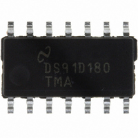
DS91D180TMA/NOPB National Semiconductor, DS91D180TMA/NOPB Datasheet

DS91D180TMA/NOPB
Specifications of DS91D180TMA/NOPB
DS91D180TMA
Available stocks
Related parts for DS91D180TMA/NOPB
DS91D180TMA/NOPB Summary of contents
Page 1
... LVDS, LV-PECL and CML) and converts them to 3V LVCMOS signals. The DS91D180 device has a M-LVDS type Typical Application in an ATCA Clock Distribution Network © 2009 National Semiconductor Corporation DS91D180/DS91C180 1 receiver input with no offset.The DS91C180 device has a type 2 receiver input which enable failsafe functionality. ...
Page 2
Connection Diagram Top View Order Number DS91D180TMA, DS91C180TMA See NS Package Number M14A Ordering Information Order Number Receiver Input DS91D180TMA DS91C180TMA M-LVDS Receiver Types The EIA/TIA-899 M-LVDS standard specifies two different types of receiver input stages. A type 1 receiver ...
Page 3
... Absolute Maximum Ratings If Military/Aerospace specified devices are required, please contact the National Semiconductor Sales Office/ Distributors for availability and specifications. Supply Voltage Control Input Voltages Driver Input Voltage Driver Output Voltages Receiver Input Voltages Receiver Output Voltage Maximum Package Power Dissipation at +25°C ...
Page 4
Symbol Parameter M-LVDS Bus (Input and Output) Pins Receiver input or driver high-impedance output A Y current Receiver input or driver high-impedance output B Z current Receiver input or driver high-impedance ...
Page 5
Switching Characteristics Over recommended operating supply and temperature ranges unless otherwise specified. Symbol Parameter DRIVER AC SPECIFICATION t Differential Propagation Delay Low to High PLH t Differential Propagation Delay High to Low PHL Pulse Skew |t − ...
Page 6
Test Circuits and Waveforms www.national.com FIGURE 2. Differential Driver Test Circuit FIGURE 3. Differential Driver Waveforms FIGURE 4. Differential Driver Full Load Test Circuit 6 20041914 20041944 20041922 ...
Page 7
FIGURE 5. Differential Driver DC Open Test Circuit FIGURE 6. Differential Driver Short-Circuit Test Circuit FIGURE 7. Driver Propagation Delay and Transition Time Test Circuit 7 20041912 20041927 20041916 www.national.com ...
Page 8
FIGURE 8. Driver Propagation Delays and Transition Time Waveforms www.national.com FIGURE 9. Driver TRI-STATE Delay Test Circuit FIGURE 10. Driver TRI-STATE Delay Waveforms 8 20041918 20041919 20041921 ...
Page 9
FIGURE 11. Receiver Propagation Delay and Transition Time Test Circuit FIGURE 12. Type 1 Receiver Propagation Delay and Transition Time Waveforms FIGURE 13. Type 2 Receiver Propagation Delay and Transition Time Waveforms 20041915 20041917 20041923 9 www.national.com ...
Page 10
FIGURE 14. Receiver TRI-STATE Delay Test Circuit FIGURE 15. Receiver TRI-STATE Delay Waveforms 10 20041913 20041920 ...
Page 11
Function Tables X — Don't care condition Z — High impedance state DS91D180 Receiving Inputs Output RE A − B ≥ 0.8V +0.05V ≤ 0.8V −0.05V 0. — Don't care condition Z — High impedance state ...
Page 12
Pin Descriptions Pin No. Name GND 13 www.national.com Description No connect. R Receiver output pin Receiver enable pin: When RE is high, the ...
Page 13
Physical Dimensions inches (millimeters) unless otherwise noted Order Number DS91D180TMA, DS91C180TMA See NS package Number M14A 13 www.national.com ...
Page 14
... For more National Semiconductor product information and proven design tools, visit the following Web sites at: Products Amplifiers www.national.com/amplifiers Audio www.national.com/audio Clock and Timing www.national.com/timing Data Converters www.national.com/adc Interface www.national.com/interface LVDS www.national.com/lvds Power Management www.national.com/power Switching Regulators www.national.com/switchers LDOs www.national.com/ldo LED Lighting www ...


