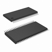
DS90CF364AMTD/NOPB National Semiconductor, DS90CF364AMTD/NOPB Datasheet - Page 5

DS90CF364AMTD/NOPB
Manufacturer Part Number
DS90CF364AMTD/NOPB
Description
IC RCVR LVDS FPD 18BIT 48-TSSOP
Manufacturer
National Semiconductor
Type
Driverr
Datasheets
1.DS90CF364AMTDNOPB.pdf
(14 pages)
2.DS90CF364MTD.pdf
(16 pages)
3.DS90CF364MTDNOPB.pdf
(16 pages)
Specifications of DS90CF364AMTD/NOPB
Number Of Drivers/receivers
1/0
Protocol
RS644
Voltage - Supply
3 V ~ 3.6 V
Mounting Type
Surface Mount
Package / Case
48-TSSOP
Number Of Drivers
21
Number Of Receivers
3
Data Rate
1300 Mbps
Operating Supply Voltage
3.3 V
Maximum Power Dissipation
1890 mW
Maximum Operating Temperature
+ 70 C
Minimum Operating Temperature
- 10 C
Mounting Style
SMD/SMT
Supply Voltage (max)
3.6 V
Supply Voltage (min)
3 V
Supply Current
60mA
Supply Voltage Range
3V To 3.6V
Driver Case Style
TSSOP
No. Of Pins
48
Operating Temperature Range
-10°C To +70°C
Msl
MSL 2 - 1 Year
Bandwidth
170GHz
Rohs Compliant
Yes
Lead Free Status / RoHS Status
Lead free / RoHS Compliant
Other names
*DS90CF364AMTD
*DS90CF364AMTD/NOPB
DS90CF364AMTD
*DS90CF364AMTD/NOPB
DS90CF364AMTD
Available stocks
Company
Part Number
Manufacturer
Quantity
Price
Company:
Part Number:
DS90CF364AMTD/NOPB
Manufacturer:
TI
Quantity:
106
CLHT
CHLT
RSPos0
RSPos1
RSPos2
RSPos3
RSPos4
RSPos5
RSPos6
RSKM
RCOP
RCOH
RCOL
RSRC
RHRC
RCCD
RPLLS
RPDD
Symbol
Receiver Switching Characteristics
Over recommended operating supply and −40°C to +85°C ranges unless otherwise specified
Note 5: Receiver Skew Margin is defined as the valid data sampling region at the receiver inputs. This margin takes into account the transmitter pulse positions
(min and max) and the receiver input setup and hold time (internal data sampling window - RSPos). This margin allows for LVDS interconnect skew, inter-symbol
interference (both dependent on type/length of cable), and clock jitter (less than 250 ps).
AC Timing Diagrams
CMOS/TTL Low-to-High Transition Time
CMOS/TTL High-to-Low Transition Time
Receiver Input Strobe Position for Bit 0
Receiver Input Strobe Position for Bit 1
Receiver Input Strobe Position for Bit 2
Receiver Input Strobe Position for Bit 3
Receiver Input Strobe Position for Bit 4
Receiver Input Strobe Position for Bit 5
Receiver Input Strobe Position for Bit 6
RxIN Skew Margin
RxCLK OUT Period
RxCLK OUT High Time
RxCLK OUT Low Time
RxOUT Setup to RxCLK OUT
RxOUT Hold to RxCLK OUT
RxCLK IN to RxCLK OUT Delay @ 25°C, V
Receiver Phase Lock Loop Set
Receiver Power Down Delay
(Note
(Figure
(Figure
(Figure 8
5)
8)
(Figure 19
(Figure 8
(Figure 16
(Figure 8
Parameter
8)
(Figure 12
)
FIGURE 1. “Worst Case” Test Pattern
)
)
)
(Figure 18
)
(Figure 4
(Figure 4
)
CC
= 3.3V
)
)
)
5
(Figure 10
f = 65 MHz
f = 65 MHz
f = 65 MHz
f = 65 MHz
f = 65 MHz
f = 65 MHz
)
11.7
13.9
3.45
Min
400
0.7
2.9
5.1
7.3
9.5
7.3
2.5
2.5
5.0
15
12.1
14.3
Typ
2.2
2.2
1.1
3.3
5.5
7.7
9.9
8.6
4.9
6.9
5.7
7.1
T
Max
10.2
12.4
14.6
1288602
5.0
5.0
1.4
3.6
5.8
8.0
9.0
50
10
1
www.national.com
Units
ms
ns
ns
ns
ns
ns
ns
ns
ns
ns
ps
ns
ns
ns
ns
ns
ns
μs


