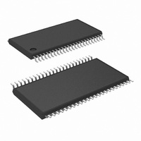
DS90CF364AMTD/NOPB National Semiconductor, DS90CF364AMTD/NOPB Datasheet - Page 14

DS90CF364AMTD/NOPB
Manufacturer Part Number
DS90CF364AMTD/NOPB
Description
IC RCVR LVDS FPD 18BIT 48-TSSOP
Manufacturer
National Semiconductor
Type
Driverr
Datasheets
1.DS90CF364AMTDNOPB.pdf
(14 pages)
2.DS90CF364MTD.pdf
(16 pages)
3.DS90CF364MTDNOPB.pdf
(16 pages)
Specifications of DS90CF364AMTD/NOPB
Number Of Drivers/receivers
1/0
Protocol
RS644
Voltage - Supply
3 V ~ 3.6 V
Mounting Type
Surface Mount
Package / Case
48-TSSOP
Number Of Drivers
21
Number Of Receivers
3
Data Rate
1300 Mbps
Operating Supply Voltage
3.3 V
Maximum Power Dissipation
1890 mW
Maximum Operating Temperature
+ 70 C
Minimum Operating Temperature
- 10 C
Mounting Style
SMD/SMT
Supply Voltage (max)
3.6 V
Supply Voltage (min)
3 V
Supply Current
60mA
Supply Voltage Range
3V To 3.6V
Driver Case Style
TSSOP
No. Of Pins
48
Operating Temperature Range
-10°C To +70°C
Msl
MSL 2 - 1 Year
Bandwidth
170GHz
Rohs Compliant
Yes
Lead Free Status / RoHS Status
Lead free / RoHS Compliant
Other names
*DS90CF364AMTD
*DS90CF364AMTD/NOPB
DS90CF364AMTD
*DS90CF364AMTD/NOPB
DS90CF364AMTD
Available stocks
Company
Part Number
Manufacturer
Quantity
Price
Company:
Part Number:
DS90CF364AMTD/NOPB
Manufacturer:
TI
Quantity:
106
www.national.com
RxIN+
RxIN−
RxOUT
RxCLK IN+
RxCLK IN−
FPSHIFT OUT
PWR DWN
V
GND
PLL V
PLL GND
LVDS V
LVDS GND
DS90CF364 Pin Description — FPD Link Receiver
Applications Information
The DS90C363 and DS90CF364 are backward compatible
with the existing 5V FPD Link transmitter/receiver pair
(DS90CF563 and DS90CF564). To upgrade from a 5V to a
3.3V system the following must be addressed:
1. Change 5V power supply to 3.3V. Provide this supply to
2. The DS90C363 (transmitter) incorporates a rise/fall
3. The DS90C363 transmitter input and control inputs ac-
CC
Pin Name
the V
and receiver devices. This change may enable the re-
moval of a 5V supply from the system, and power may
be supplied from an existing 3V power source.
strobe select pin. This select function is on pin 14, for-
merly a V
rise/fall strobe select pin is connected to V
configured with a rising edge strobe. In a system cur-
rently using a 5V rising edge strobe transmitter
(DS90CR563), no layout changes are required to ac-
commodate the new rise/fall select pin on the 3.3V
transmitter. The V
the device will be configured with a rising edge strobe.
When converting from a 5V falling edge transmitter
(DS90CF563) to the 3V transmitter a minimal board
layout change is necessary. The 3.3V transmitter will
not be configured with a falling edge strobe if V
mains connected to the select pin. To guarantee the
3.3V transmitter functions with a falling edge strobe pin
14 should be connected to ground OR left unconnected.
When not connected (left open) and internal pull-down
resistor ties pin 14 to ground, thus configuring the trans-
mitter with a falling edge strobe.
cept 3.3V TTL/CMOS levels. They are not 5V tolerant.
CC
CC
CC
, LVDS V
CC
connection on the 5V products. When the
I/O
O
O
CC
I
I
I
I
I
I
I
I
I
I
I
CC
and PLL V
No.
signal may remain at pin 14, and
21
3
3
1
1
1
1
4
5
1
2
1
3
Positive LVDS differentiaI data inputs.
Negative LVDS differential data inputs.
TTL level data outputs. This includes: 6 Red, 6 Green, 6 Blue, and 3 control lines — FPLINE,
FPFRAME, DRDY (also referred to as HSYNC, VSYNC, Data Enable).
Positive LVDS differential clock input.
Negative LVDS differential clock input.
TTL Ievel clock output. The falling edge acts as data strobe. Pin name RxCLK OUT.
TTL level input. When asserted (low input) the receiver outputs are low.
Power supply pins for TTL outputs.
Ground pins for TTL outputs.
Power supply for PLL.
Ground pin for PLL.
Power supply pin for LVDS inputs.
Ground pins for LVDS inputs.
CC
of both the transmitter
CC
, the part is
CC
re-
14
Description


