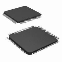
DS90C387AVJD/NOPB National Semiconductor, DS90C387AVJD/NOPB Datasheet - Page 12

DS90C387AVJD/NOPB
Manufacturer Part Number
DS90C387AVJD/NOPB
Description
IC RCVR/TX DUAL LVDS FPD 100TQFP
Manufacturer
National Semiconductor
Type
Transceiverr
Datasheet
1.DS90C387AVJDNOPB.pdf
(19 pages)
Specifications of DS90C387AVJD/NOPB
Number Of Drivers/receivers
8/0
Protocol
RS644
Voltage - Supply
3 V ~ 3.6 V
Mounting Type
Surface Mount
Package / Case
100-TQFP, 100-VQFP
Supply Voltage Range
3V To 3.6V
Operating Temperature Range
-10°C To +70°C
Audio Ic Case Style
TQFP
No. Of Pins
100
Svhc
No SVHC (15-Dec-2010)
Base Number
90
Rohs Compliant
Yes
Data Rate
5700Mbps
Interface Type
LVDS
Number Of Drivers
2
Number Of Receivers
48
Operating Supply Voltage
3.3 V
Maximum Power Dissipation
2800 mW
Maximum Operating Temperature
+ 70 C
Minimum Operating Temperature
- 10 C
Mounting Style
SMD/SMT
Supply Voltage (max)
3.6 V
Supply Voltage (min)
3 V
Lead Free Status / RoHS Status
Lead free / RoHS Compliant
Other names
*DS90C387AVJD
*DS90C387AVJD/NOPB
DS90C387AVJD
*DS90C387AVJD/NOPB
DS90C387AVJD
Available stocks
Company
Part Number
Manufacturer
Quantity
Price
Company:
Part Number:
DS90C387AVJD/NOPB
Manufacturer:
Texas Instruments
Quantity:
10 000
www.national.com
DS90C387A Pin Descriptions — FPD Link Transmitter
Note 10: Inputs default to “low” when left open due to internal pull-down resistor.
Note 11: The PLL range shift point is in the 55 - 68 MHz range, typically the shift will occur during the lock time.
Rn, Gn, Bn,
DE, HSYNC,
VSYNC
AnP
AnM
CLKIN
R_FB
R_FDE
CLK1P
CLK1M
PD
PLLSEL
PRE
DUAL
V
GND
PLLV
PLLGND
LVDSV
LVDSGND
CLK2P/NC
CLK2M/NC
CC
Pin Name
CC
CC
I/O
O
O
O
O
O
O
I
I
I
I
I
I
I
I
I
I
I
I
I
I
No.
51
8
8
1
1
1
1
1
1
1
1
1
4
6
2
3
3
4
1
1
TTL level input. This includes: 16 Red, 16 Green, 16 Blue, and 3 control
lines HSYNC, VSYNC, DE (Data Enable).(Note 10)
Positive LVDS differential data output.
Negative LVDS differential data output.
TTL level clock input.
Programmable data strobe select. Rising data strobe edge selected when
input is high. (Note 10)
Programmable control (DE) strobe select. Tied high for data active when DE
is high. (Note 10)
Positive LVDS differential clock output.
Negative LVDS differential clock output.
TTL level input. Assertion (low input) tri-states the outputs, ensuring low
current at power down. (Note 10)
PLL range select. This pin must be tied to V
Ground is reserved for future use. Typical shift point is between 55 and 68
MHz. (Notes 10, 11)
Pre-emphasis level select. Pre-emphasis is active when input is tied to V
through external pull-up resistor. Resistor value determines pre-emphasis
level (see table in application section). For normal LVDS drive level (No
pre-emphasis) leave this pin open (do not tie to ground).(Note 10)
Three-mode select for dual pixel, single pixel, or single pixel input to dual
pixel output operation. Single pixel mode when input is low (only LVDS
channels A0 thru A3 and CLK1 are active) for power savings. Dual mode is
active when input is high. Single in - dual out when input is at 1/2 Vcc. (Note
10)
Power supply pins for TTL inputs and digital circuitry.
Ground pins for TTL inputs and digital circuitry.
Power supply pin for PLL circuitry.
Ground pins for PLL circuitry.
Power supply pin for LVDS outputs.
Ground pins for LVDS outputs.
Additional positive LVDS differential clock output. Identical to CLK1P. No
connect if not used.
Additional negative LVDS differential clock output. Identical to CLK1M. No
connect if not used.
12
Description
CC
for auto-range. NC or tied to
CC


