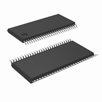
DS90CR288AMTD/NOPB National Semiconductor, DS90CR288AMTD/NOPB Datasheet - Page 4

DS90CR288AMTD/NOPB
Manufacturer Part Number
DS90CR288AMTD/NOPB
Description
IC RCVR 28BIT CHAN LINK 56TSSOP
Manufacturer
National Semiconductor
Type
Receiverr
Datasheet
1.DS90CR287MTDNOPB.pdf
(16 pages)
Specifications of DS90CR288AMTD/NOPB
Number Of Drivers/receivers
0/4
Protocol
RS644
Voltage - Supply
3 V ~ 3.6 V
Mounting Type
Surface Mount
Package / Case
56-TSSOP
Supply Current
135mA
Supply Voltage Range
3V To 3.6V
Driver Case Style
TSSOP
No. Of Pins
56
Operating Temperature Range
-10°C To +70°C
Msl
MSL 2 - 1 Year
Data Rate Max
595Mbps
Rohs Compliant
Yes
Lead Free Status / RoHS Status
Lead free / RoHS Compliant
Other names
*DS90CR288AMTD
*DS90CR288AMTD/NOPB
DS90CR288AMTD
*DS90CR288AMTD/NOPB
DS90CR288AMTD
Available stocks
Company
Part Number
Manufacturer
Quantity
Price
Company:
Part Number:
DS90CR288AMTD/NOPB
Manufacturer:
TI
Quantity:
2 100
www.national.com
LLHT
LHLT
TCIT
TPPos0
TPPos1
TPPos2
TPPos3
TPPos4
TPPos5
TPPos6
TCIP
TCIH
TCIL
TSTC
THTC
TCCD
TPLLS
TPDD
TJIT
Symbol
Electrical Characteristics
TRANSMITTER SUPPLY CURRENT
I
I
RECEIVER SUPPLY CURRENT
I
Symbol
Note 1: “Absolute Maximum Ratings” are those values beyond which the safety of the device cannot be guaranteed. They are not meant to imply that the device
should be operated at these limits. The tables of “Electrical Characteristics” specify conditions for device operation.
Note 2: Typical values are given for V
Note 3: Current into device pins is defined as positive. Current out of device pins is defined as negative. Voltages are referenced to ground unless otherwise
specified (except V
Note 4: V
Transmitter Switching Characteristics
Over recommended operating supply and temperature ranges unless otherwise specified
I
CCTW
CCTZ
CCRZ
CCRW
Over recommended operating supply and temperature ranges unless otherwise specified
OS
previously referred as V
Transmitter Supply Current Worst
Case (with Loads)
Transmitter Supply Current Power
Down
Receiver Supply Current Worst
Case
Receiver Supply Current Power
Down
LVDS Low-to-High Transition Time (Figure 2)
LVDS High-to-Low Transition Time (Figure 2)
TxCLK IN Transition Time (Figure 4)
Transmitter Output Pulse Position for Bit0 (Figure 14)
Transmitter Output Pulse Position for Bit1
Transmitter Output Pulse Position for Bit2
Transmitter Output Pulse Position for Bit3
Transmitter Output Pulse Position for Bit4
Transmitter Output Pulse Position for Bit5
Transmitter Output Pulse Position for Bit6
TxCLK IN Period (Figure 5 )
TxCLK IN High Time (Figure 5)
TxCLK IN Low Time (Figure 5)
TxIN Setup to TxCLK IN (Figure 5)
TxIN Hold to TxCLK IN (Figure 5)
TxCLK IN to TxCLK OUT Delay (Figure 7)
Transmitter Phase Lock Loop Set (Figure 9)
Transmitter Powerdown Delay (Figure 12)
TxCLK IN Cycle-to-Cycle Jitter (Input clock requirement)
OD
and ∆V
Parameter
OD
).
CM
CC
.
= 3.3V and T
A
(Continued)
= +25˚C.
Parameter
R
C
Worst Case
Pattern
(Figures 1, 2)
PWR DWN = Low
Driver Outputs in TRI-STATE
under Powerdown Mode
C
Worst Case
Pattern
(Figures 1, 3)
PWR DWN = Low
Receiver Outputs Stay Low during
Powerdown Mode
L
L
L
= 100Ω,
= 5 pF,
= 8 pF,
4
Conditions
f = 33 MHz
f = 40 MHz
f = 66 MHz
f = 85 MHz
f = 33 MHz
f = 40 MHz
f = 66 MHz
f = 85 MHz
f = 85 MHz
f = 85 MHz
T
V
A
CC
= 25˚C,
= 3.3V
0.35T
0.35T
−0.20
11.76
1.48
3.16
4.84
6.52
8.20
9.88
Min
1.0
2.5
3.8
Min
0
10.08
0.75
0.75
1.68
3.36
5.04
6.72
8.40
0.5T
0.5T
Typ
Typ
140
31
32
37
42
10
49
53
81
96
0
T
10.28
0.65T
0.65T
Max
Max
0.20
1.88
3.56
5.24
6.92
8.60
114
135
400
100
1.5
1.5
6.0
6.3
45
50
55
60
55
70
75
50
10
2
Units
Units
mA
mA
mA
mA
mA
mA
mA
mA
µA
µA
ms
ns
ns
ns
ns
ns
ns
ns
ns
ns
ns
ns
ns
ns
ns
ns
ns
ns
ns


