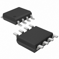
MAX13487EESA+ Maxim Integrated Products, MAX13487EESA+ Datasheet - Page 11

MAX13487EESA+
Manufacturer Part Number
MAX13487EESA+
Description
IC TXRX RS485/422 8-SOIC
Manufacturer
Maxim Integrated Products
Type
Transceiverr
Datasheet
1.MAX13487EESA.pdf
(17 pages)
Specifications of MAX13487EESA+
Number Of Drivers/receivers
1/1
Protocol
RS422, RS485
Voltage - Supply
4.75 V ~ 5.25 V
Mounting Type
Surface Mount
Package / Case
8-SOIC (3.9mm Width)
Data Rate
0.5 Mbps
Operating Supply Voltage
5 V
Supply Current
4.5 mA
Operating Temperature Range
- 40 C to + 125 C
Maximum Power Dissipation
471 mW
Mounting Style
SMD/SMT
Lead Free Status / RoHS Status
Lead free / RoHS Compliant
X = Don’t care, shutdown mode, driver, and receiver outputs are in high impedance.
PIN
1
2
3
4
5
6
7
8
SHDN
SHDN
1
1
1
1
0
1
1
1
1
1
0
NAME
SHDN
GND
V
RO
RE
DI
A
B
CC
______________________________________________________________________________________
RE
DI
0
1
1
1
X
0
0
1
1
1
X
Half-Duplex RS-485-/RS-422-Compatible
Transceiver with AutoDirection Control
Receiver Output. When receiver is enabled and V(A) - V(B) > +200mV, RO is high. If V(A) - V(B)
< -200mV, RO is low.
Receiver Output Enable. Drive RE low to enable the RO. Drive RE high to let the AutoDirection circuit
control the receiver. RE is a hot-swap input (see the Hot-Swap Capability section for more details).
Shutdown. Drive SHDN high to let the device operate in normal operation. Drive SHDN low to put the part
in shutdown.
Driver Input. Drive DI low to force noninverting output low and inverting output high. Drive DI high to force
noninverting output high and inverting output low. DI is an input to the internal state machine that
automatically enables and disables the driver. See the Function Tables and General Description for more
information. DI is a hot-swap input (see the Hot-Swap Capability section for more details).
Ground
Noninverting Receiver Input and Noninverting Driver Output
Inverting Receiver Input and Inverting Driver Output
Positive Supply, V
A-B > V
≥+200mV
≥+200mV
≤-200mV
≤-200mV
False
False
INPUTS
True
A-B
X
X
X
X
DT
CC
= +5V ±5%. Bypass V
INPUTS
If driver was OFF, keep it OFF
If driver was ON, keep it ON
DRIVER STATE
Turn driver OFF
Turn driver ON
TRANSMITTING
OFF
OFF
ON
RECEIVING
ACTION
X
X
X
X
CC
to GND with a 0.1µF capacitor.
FUNCTION
RECEIVER STATE
HIGH IMPEDANCE
HIGH IMPEDANCE
OFF
ON
ON
ON
ON
X
A
0
1
SHUTDOWN
OUTPUTS
Function Tables
Pin Description
HIGH IMPEDANCE
HIGH IMPEDANCE
HIGH IMPEDANCE
SHUTDOWN
OUTPUT
RO
1
0
1
0
B
1
0
11


