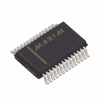
MAX213EEAI+ Maxim Integrated Products, MAX213EEAI+ Datasheet - Page 8

MAX213EEAI+
Manufacturer Part Number
MAX213EEAI+
Description
IC TXRX RS232 5V 28-SSOP
Manufacturer
Maxim Integrated Products
Type
Transceiverr
Specifications of MAX213EEAI+
Number Of Drivers/receivers
4/5
Protocol
RS232
Voltage - Supply
4.5 V ~ 5.5 V
Mounting Type
Surface Mount
Package / Case
28-SSOP
Supply Voltage (max)
5.5 V
Supply Voltage (min)
4.5 V
Maximum Operating Temperature
+ 85 C
Mounting Style
SMD/SMT
Data Rate
120 Kbps
Interface
RS-232
Maximum Power Dissipation
762 mW
Minimum Operating Temperature
- 40 C
Propagation Delay Time
0.5 us
Supply Current
14 mA
Operating Supply Voltage
5 V
Operating Temperature Range
- 40 C to + 85 C
Dimensions
10.33 mm L x 5.38 mm W x 1.99 mm H
Lead Free Status / RoHS Status
Lead free / RoHS Compliant
+5V, RS-232 Transceivers
with 0.1µF External Capacitors
The type of capacitor used is not critical for proper
operation. Ceramic capacitors are suggested. To ensure
proper RS-232 signal levels over temperature when
using 0.1FF capacitors, make sure the capacitance
value does not degrade excessively as the temperature
varies. If in doubt, use capacitors with a larger nominal
value. Also observe the capacitors’ ESR value over tem-
perature, since it influences the amount of ripple on V+
and V-. To reduce the output impedance at V+ and V-,
use larger capacitors (up to 10FF). If polarized capaci-
tors are used, obey the polarities shown in Figure 1 and
the pin configurations.
Each transmitter is designed to drive a single receiver.
Transmitters can be paralleled to drive multiple receivers.
Table 3. DB9 Cable Connections Commonly Used for EIA/TIA-232E and V.24
Asynchronous Interfaces
8
Table 2. Summary of EIA/TIA-232E, V.28 Specifications
Driver Output Voltage: 0 Level
Driver Output Voltage: 1 Level
Output Level, Maximum
Data Rate
Receiver Input Voltage: 0 Level
Receiver Input Voltage: 1 Level
Input Level, Maximum
Instantaneous Slew Rate, Maximum
Driver Output Short-Circuit Current, Maximum
Transition Rate on Driver Output
Driver Output Resistance
PIN
1
2
3
4
5
6
7
8
9
Received Line Signal Detector, sometimes called Carrier Detect (DCD)
Receive Data (RD)
Transmit Data (TD)
Data Terminal Ready
Signal Ground
Data Set Ready (DSR)
Request to Send (RTS)
Clear to Send (CTS)
Ring Indicator
PARAMETER
Applications Information
Driving Multiple Receivers
Capacitor Selection
NAME
3kI P R
3kI P R
-2V < V
3kI to 7kI load
3kI to 7kI load
L
L
EIA/TIA-232E
CONDITION
P 7kI, C
P 7kI, C
No load
V.28
OUT
—
—
—
—
Figure 5 shows two driver outputs exiting shutdown. As
they become active, the two driver outputs go to oppo-
site RS-232 levels (one driver input is high, the other
is low). Each driver is loaded with 3kI in parallel with
2500pF. The driver outputs display no ringing or undesir-
able transients as they come out of shutdown.
In applications that are sensitive to power-supply noise,
decouple V
value as the charge-pump capacitors.
A small amount of power can be drawn from V+ and V-,
although this reduces noise margins.
If at power-up the V+ supply rises after the V
place a diode (e.g., 1N914) in series with the V+ supply.
< +2V
L
L
P 2500pF
P 2500pF
Driver Outputs When Exiting Shutdown
Power Supplies for MAX201/MAX209
CC
to ground with a capacitor of the same
V+ and V- as Power Supplies
EIA/TIA-232E, V.28 SPECIFICATION
Reference point for signals
Power-Supply Decoupling
Handshake from DCE
Handshake from DCE
Handshake from DCE
Handshake from DCE
Handshake from DTE
Handshake from DTE
1ms or 3% of the period
CONNECTION
Data from DCE
Data from DTE
4% of the period
+5.0V to +15V
+3.0V to +15V
Up to 20kbps
-5.0V to -15V
-3.0V to -15V
100mA
30V/Fs
Q25V
Q25V
300I
CC
supply,


