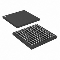
DS3251+ Maxim Integrated Products, DS3251+ Datasheet - Page 49

DS3251+
Manufacturer Part Number
DS3251+
Description
IC LIU DS3/E3/STS-1 144-CSBGA
Manufacturer
Maxim Integrated Products
Type
Line Interface Units (LIUs)r
Specifications of DS3251+
Number Of Drivers/receivers
1/1
Protocol
DS3
Voltage - Supply
3.135 V ~ 3.465 V
Mounting Type
Surface Mount
Package / Case
144-CSBGA
Lead Free Status / RoHS Status
Lead free / RoHS Compliant
Table 17-H. Parallel CPU Interface Timing
(V
Setup Time for A[5:0] Valid to CS Active (Notes 1, 2)
Setup Time for CS Active to RD, WR, or DS Active
Delay Time from RD or DS Active to D[7:0] Valid
Hold Time from RD or WR or DS Inactive to CS Inactive
Delay from CS or RD or DS Inactive to D[7:0] Invalid or Tri-
State (Note 3)
Wait Time from WR or DS Active to Latch D[7:0]
D[7:0] Setup Time to WR or DS Inactive
D[7:0] Hold Time from WR or DS Inactive
A[5:0] Hold Time from WR or RD or DS Inactive
RD, WR, or DS Inactive Time
Muxed Address Valid to ALE Falling (Note 4)
Muxed Address Hold Time (Note 4)
ALE Pulse Width (Note 4)
Setup Time for ALE High or Muxed Address Valid to CS
Active (Note 4)
Note 1:
Note 2:
Note 3:
Note 4:
DD
= 3.3V ±5%, T
D[7:0] loaded with 50pF when tested as outputs.
If a gapped clock is applied on TCLK and local loopback is enabled, read cycle time must be extended by the length of the largest
TCLK gap.
Not tested during production test.
In nonmultiplexed bus applications
should be wired to D[5:0] and the falling edge of ALE latches the address.
A
= -40°C to +85°C.)
PARAMETER
(Figure
(Figure 17-3
17-3), ALE should be wired high. In multiplexed bus applications
and
49 of 71
Figure
SYMBOL
17-4)
t10
t11
t12
t13
t14
t1
t2
t3
t4
t5
t6
t7
t8
t9
MIN
65
10
75
10
10
30
0
0
0
2
2
5
0
TYP
MAX
(Figure
65
20
17-4), A[5:0]
UNITS
ns
ns
ns
ns
ns
ns
ns
ns
ns
ns
ns
ns
ns
ns


