AMIS-49250-XTD ON Semiconductor, AMIS-49250-XTD Datasheet - Page 17

AMIS-49250-XTD
Manufacturer Part Number
AMIS-49250-XTD
Description
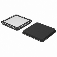
IC TXRX FIELDBUS MAU 44-NQFP
Manufacturer
ON Semiconductor
Type
Transceiverr
Datasheet
1.AMIS-49200-XTD.pdf
(22 pages)
Specifications of AMIS-49250-XTD
Number Of Drivers/receivers
1/1
Protocol
MDS-MAU
Voltage - Supply
4.75 V ~ 6.2 V
Mounting Type
Surface Mount
Package / Case
44-LQFP
Logic Type
Fieldbus Media Access Unit
Logic Family
AMIS-492x0
Number Of Channels Per Chip
1
Input Level
CMOS
Output Level
CMOS
Output Type
Open Drain
High Level Output Current
50 uA
Low Level Output Current
50 uA
Supply Voltage (max)
6.2 V
Supply Voltage (min)
3 V
Maximum Operating Temperature
+ 85 C
Minimum Operating Temperature
- 40 C
Mounting Style
SMD/SMT
Polarity
Inverting/Non-Inverting
Number Of Transmitters
1
Power Supply Requirement
Dual
Operating Temperature Classification
Industrial
Mounting
Surface Mount
Pin Count
44
Operating Temperature (max)
85C
Operating Temperature (min)
-40C
Lead Free Status / RoHS Status
Lead free / RoHS Compliant
Other names
AMIS-49250-XTDOS
Available stocks
Company
Part Number
Manufacturer
Quantity
Price
Company:
Part Number:
AMIS-49250-XTD
Manufacturer:
ON Semiconductor
Quantity:
10 000
AMIS-492x0
4.4.2. Receive Signal Detection
The carrier detector generates the receive activity (RxA) signal by detecting the input signal amplitude. Minimum amplitude is 100mVp-
p (TYP). A delay, determined by the capacitor connected between the CCD pin and GND, is added to avoid detection of transient
noise. The recommended value of C
The zero-cross detector generates the receive signal (RxS) with minimum phase error (jitter) by detecting the transition between high
and low levels of the incoming Manchester code. Hysteresis of +40mV (TYP) is applied to avoid unnecessary switching by noise.
Once the carrier-detect goes active the hysteresis is removed and the switching point threshold is set to Vmid. The output can drive a
CMOS input of V
DD
supply voltage.
Detectors
35
34
CCD
32
RXA
RXS
To
Convert
Level
Convert
VDD
Level
VDD
31
FLTOUT
CD
CD_Output
VCC
is 100pF. The output can drive a CMOS input of V
VCC
A2
VCC
C3=220pf
C1
29
Carrier Detector
C4=47pf
ZC Tript Pt
Rev. 6 | Page 17 of 22 | www.onsemi.com
RF4
54K
Figure 12: Receive Signal Detectors
30
Figure 11: Band Pass Filter
VCC
VCC
FLT
Vtrip = Vmid
Vhyst = + 40mV
RF3
20K
Zero-Cross Detector
C2
C2
VHi50
VLo50
VCC
A1
RF1
75K
Bandpass Filter
270K
RF2
RxSig
VHi50 = Vmid + 50mV
VLo50 = Vmid - 50mV
Vmid
HPF
SIGIN
28
27
R
(1Meg)
Vmid
(60pF)
DD
1000pf
C
C2
supply voltage.
Filtered received signal
from Bandpass Filter
1000pf
C1
Signal
Input


