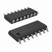
DS34C86TM/NOPB National Semiconductor, DS34C86TM/NOPB Datasheet - Page 2

DS34C86TM/NOPB
Manufacturer Part Number
DS34C86TM/NOPB
Description
IC LINE RCVR QUAD CMOS 16-SOIC
Manufacturer
National Semiconductor
Type
Receiverr
Datasheet
1.DS34C86TMXNOPB.pdf
(8 pages)
Specifications of DS34C86TM/NOPB
Number Of Drivers/receivers
0/4
Protocol
RS422, RS423
Voltage - Supply
4.5 V ~ 5.5 V
Mounting Type
Surface Mount
Package / Case
16-SOIC (3.9mm Width)
Number Of Receivers
4
Number Of Transmitters
Not Required
Number Of Transceivers
Not Required
Data Transmission Topology
Multidrop
Receiver Signal Type
Differential
Transmitter Signal Type
Not Required
Single Supply Voltage (typ)
5V
Single Supply Voltage (min)
4.5V
Single Supply Voltage (max)
5.5V
Dual Supply Voltage (typ)
Not RequiredV
Dual Supply Voltage (min)
Not RequiredV
Dual Supply Voltage (max)
Not RequiredV
Supply Current
23mA
Power Supply Requirement
Single
Operating Temp Range
-40C to 85C
Operating Temperature Classification
Industrial
Mounting
Surface Mount
Pin Count
16
Package Type
SOIC N
Lead Free Status / RoHS Status
Lead free / RoHS Compliant
Other names
*DS34C86TM
DS34C86TM
DS34C86TM
Available stocks
Company
Part Number
Manufacturer
Quantity
Price
www.national.com
V
R
I
V
V
V
V
I
I
I
V
t
t
t
t
t
t
IN
OZ
I
CC
PLH
PHL
RISE
FALL
PLZ
PHZ
TH
IN
OH
OL
IH
IL
HYST
Absolute Maximum Ratings
2)
If Military/Aerospace specified devices are required,
please contact the National Semiconductor Sales Office/
Distributors for availability and specifications.
DC Electrical Characteristics
V
Symbol
AC Electrical Characteristics
V
CC
CC
,
,
Symbol
,
= 5V
= 5V
Supply Voltage (V
Input Common Mode Range (V
CM
Differential Input Voltage (V
DIFF
Enable Input Voltage (V
Storage Temperature Range (T
STG
Lead Temperature (Soldering 4
sec)
)
)
)
±
±
Minimum Differential
Input Voltage
Input Resistance
Input Current
(Under Test)
Minimum High Level
Output Voltage
Maximum Low Level
Output Voltage
Minimum Enable High
Input Level Voltage
Maximum Enable Low
Input Level Voltage
Maximum TRI-STATE
Output Leakage Current
Maximum Enable Input
Current
Quiescent Power
Supply Current
Input Hysteresis
10% (unless otherwise specified)
10% (unless otherwise specified) (Figures 1, 2, 3)
Propagation Delay
Input to Output
Output Rise and
Fall Times
Propagation Delay
ENABLE to Output
Parameter
CC
)
Parameter
IN)
V
−7V
V
(Other Input = GND)
V
V
V
I
V
I
V
TRI-STATE Control = V
V
V
V
OUT
OUT
OUT
IN
IN
IN
CC
CC
OUT
IN
CC
CM
−65˚C to
+150˚C
(Notes 1,
C
V
V
C
V
V
C
R
= V
= −7V, +7V
= +10V, Other Input = GND
= −10V, Other Input = GND
260˚C
DIFF
CM
DIFF
CM
±
±
<
= Min., V
= Max., V
= Max., V
L
L
L
L
= −6.0 mA
= 6.0 mA
= 0V
(Note 3)
(Note 3)
= V
= V
14V
14V
= 50 pF
= 50 pF
= 50 pF
= 1000Ω
V
7V
7V
CC
= 0V
= 0V
CM
Conditions
= 2.5V
= 2.5V
OH
CC
or GND
<
or GND,
or V
(DIFF)
Conditions
+7V
(DIFF)
(DIFF)
OL
2
= +1V
= −1V
= +1V
This device does not meet 2000V ESD rating. (Note 4)
Operating Conditions
IL
Supply Voltage (V
Operating Temperature Range (T
Enable Input Rise or Fall Times
Maximum Power Dissipation at 25˚C (Note 5)
Current Per Output
Plastic “N” Package
SOIC Package
Min
CC
−200
Min
5.0
3.8
2.0
)
Typ
19
13
4
+1.1
−2.0
±
Typ
6.8
4.2
0.2
35
16
60
0.5
A
)
Max
30
18
9
4.50
Min
−40
+200
+1.5
−2.5
±
±
Max
0.3
0.8
10
23
5.0
1.0
1645 mW
1190 mW
±
Max
5.50
+85
500
25 mA
Units
ns
ns
ns
Unit
Units
˚C
ns
mV
mA
mA
mA
mV
V
kΩ
µA
µA
V
V
V
V


