MAX3450EEUD+ Maxim Integrated Products, MAX3450EEUD+ Datasheet - Page 2
MAX3450EEUD+
Manufacturer Part Number
MAX3450EEUD+
Description
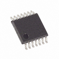
TXRX USB +/-15KV ESD 14-TSSOP
Manufacturer
Maxim Integrated Products
Type
Transceiverr
Datasheet
1.MAX3451EEUD.pdf
(14 pages)
Specifications of MAX3450EEUD+
Number Of Drivers/receivers
1/1
Protocol
USB 2.0
Voltage - Supply
3 V ~ 3.6 V
Mounting Type
Surface Mount
Package / Case
14-TSSOP
Lead Free Status / RoHS Status
Lead free / RoHS Compliant


±15kV ESD-Protected USB Transceivers
ABSOLUTE MAXIMUM RATINGS
V
V
VP, VM, SUS, SPD, ENUM,
Current (into any pin)........................................................±15mA
Short-Circuit Current (D+ and D-) ..................................±150mA
Continuous Power Dissipation (T
DC ELECTRICAL CHARACTERISTICS
(V
are at V
Note 1: Package thermal resistances were obtained using the method described in JEDEC specifications. For detailed information
on package thermal considerations, refer to www.maxim-ic.com/thermal-tutorial.
Stresses beyond those listed under “Absolute Maximum Ratings” may cause permanent damage to the device. These are stress ratings only, and functional
operation of the device at these or any other conditions beyond those indicated in the operational sections of the specifications is not implied. Exposure to
absolute maximum rating conditions for extended periods may affect device reliability.
2
SUPPLY INPUTS (V
Regulated Supply Voltage
Output
Operating Supply Current
Operating V
Full-Speed Idle and SE0 Supply
Current
Static V
Suspend Supply Current
Disable-Mode Supply Current
Sharing-Mode V
Current
D+/D- Sharing-Mode
Load Current
D+/D- Disable-Mode
Load Current
BUS
TRM
BUS
RCV, OE, BD to GND ................................-0.3V to (V
14-Pin TSSOP
(derate 10mW/°C above +70°C) ..................................797mW
16-Pin Thin QFN-EP 3mm x 3mm
(derate 20.8mW/°C above +70°C) .............................1667mW
_______________________________________________________________________________________
, V
to GND ............................................-0.3V to (V
= +4.0V to +5.5V or V
BUS
L
L
, D+, D- to GND.......................................-0.3V to +6.0V
PARAMETER
Supply Current
= +5.0V, V
L
Supply Current
L
Supply
BUS
L
= +2.5V, and T
, V
TRM
TRM
A
, V
= +3.0V to +3.6V, V
= +70°C)
L
I
I
I
VL(SHARING)
D_(SHARING)
I
)
I
VBUS(SUSP)
I
VBUS(IDLE)
VL(STATIC)
SYM B O L
VBUS(DIS)
I
D_(DIS)
I
V
VBUS
A
I
TRM
VL
= +25°C.) (Note 2)
Internal regulator
Full-speed transmitting/receiving at 12Mbps,
C
Full-speed transmitting/receiving at 12Mbps
(Note 3)
Full-speed idle: V
SE0: V
Full-speed idle,
SE0, or suspend
mode
VM = VP = open,
SUS = OE = high
V
V
OE = low, VP = low or
high, VM = low or
high, SUS = high
V
V
L
BUS
BUS
L
L
BUS
= GND or open
= GND or open, V
= 50pF on D+ and D- (Note 3)
L
L
= +1.65V to +3.6V, T
= GND or open,
= GND or open, V
+ 0.3V)
+ 0.3V)
D+
< 0.3V, V
CONDITIONS
D+
D-
Package Junction-to-Ambient Thermal Resistance (θ
Package Junction-to-Case Thermal Resistance (θ
Operating Temperature Range ...........................-40°C to +85°C
Junction Temperature ......................................................+150°C
Storage Temperature Range .............................-65°C to +150°C
Lead Temperature (soldering, 10s) .................................+300°C
> 2.7V, V
D_
< 0.3V
14-Pin TSSOP..........................................................100.4°C/W
16-Pin Thin QFN-EP .....................................................48°C/W
14-Pin TSSOP...............................................................30°C/W
16-Pin Thin QFN-EP .......................................................7°C/W
D_
= 0 or +5.5V
MAX3450E,
MAX3451E
MAX3452E
MAX3450E,
MAX3451E
(ENUM = low)
MAX3452E
MAX3450E,
MAX3451E
MAX3452E
A
= 0 or +5.5V
= T
D-
MIN
< 0.3V
to T
MAX
, unless otherwise noted. Typical values
MIN
3.0
TYP
250
250
3.3
MAX
350
350
3.6
2.5
10
15
35
40
20
20
20
JC
5
5
5
) (Note 1)
JA
) (Note 1)
UNITS
mA
mA
µA
µA
µA
µA
µA
µA
µA
V
Related parts for MAX3450EEUD+
Image
Part Number
Description
Manufacturer
Datasheet
Request
R

Part Number:
Description:
�15kV ESD-Protected USB Transceivers
Manufacturer:
MAXIM [Maxim Integrated Products]
Datasheet:

Part Number:
Description:
MAX7528KCWPMaxim Integrated Products [CMOS Dual 8-Bit Buffered Multiplying DACs]
Manufacturer:
Maxim Integrated Products
Datasheet:
Part Number:
Description:
Single +5V, fully integrated, 1.25Gbps laser diode driver.
Manufacturer:
Maxim Integrated Products
Datasheet:
Part Number:
Description:
Single +5V, fully integrated, 155Mbps laser diode driver.
Manufacturer:
Maxim Integrated Products
Datasheet:
Part Number:
Description:
VRD11/VRD10, K8 Rev F 2/3/4-Phase PWM Controllers with Integrated Dual MOSFET Drivers
Manufacturer:
Maxim Integrated Products
Datasheet:
Part Number:
Description:
Highly Integrated Level 2 SMBus Battery Chargers
Manufacturer:
Maxim Integrated Products
Datasheet:
Part Number:
Description:
Current Monitor and Accumulator with Integrated Sense Resistor; ; Temperature Range: -40°C to +85°C
Manufacturer:
Maxim Integrated Products
Part Number:
Description:
TSSOP 14/A�/RS-485 Transceivers with Integrated 100O/120O Termination Resis
Manufacturer:
Maxim Integrated Products
Part Number:
Description:
TSSOP 14/A�/RS-485 Transceivers with Integrated 100O/120O Termination Resis
Manufacturer:
Maxim Integrated Products
Part Number:
Description:
QFN 16/A�/AC-DC and DC-DC Peak-Current-Mode Converters with Integrated Step
Manufacturer:
Maxim Integrated Products
Part Number:
Description:
TDFN/A/65V, 1A, 600KHZ, SYNCHRONOUS STEP-DOWN REGULATOR WITH INTEGRATED SWI
Manufacturer:
Maxim Integrated Products
Part Number:
Description:
Integrated Temperature Controller f
Manufacturer:
Maxim Integrated Products
Part Number:
Description:
SOT23-6/I�/45MHz to 650MHz, Integrated IF VCOs with Differential Output
Manufacturer:
Maxim Integrated Products
Part Number:
Description:
SOT23-6/I�/45MHz to 650MHz, Integrated IF VCOs with Differential Output
Manufacturer:
Maxim Integrated Products
Part Number:
Description:
EVALUATION KIT/2.4GHZ TO 2.5GHZ 802.11G/B RF TRANSCEIVER WITH INTEGRATED PA
Manufacturer:
Maxim Integrated Products